Supercharge Your Innovation With Domain-Expert AI Agents!

Flip Chip Stacked Package

A flip-chip and chip technology, applied to electrical components, electrical solid devices, circuits, etc., can solve the problems of poor heat dissipation efficiency of the bottom chip, and achieve the effects of improving heat dissipation efficiency, reducing manufacturing costs, and simple structure

Inactive Publication Date: 2015-08-26
CHIPMOS TECH INC
View PDF4 Cites 5 Cited by
  • Summary
  • Abstract
  • Description
  • Claims
  • Application Information

AI Technical Summary

Problems solved by technology

[0003] The heat dissipation method of the known semiconductor package usually adds a heat sink outside the package, such as a heat dissipation metal sheet arranged outside the package to meet the heat dissipation requirements. However, when this heat dissipation method is applied to the package structure of stacked chips, the bottom layer The heat dissipation efficiency of the chip is poorer than that of the top chip

Method used


Image

  • Flip Chip Stacked Package
  • Flip Chip Stacked Package
  • Flip Chip Stacked Package

Examples


Embodiment Construction

[0039] In order to make the advantages, spirit and characteristics of the present invention more easily and clearly understood, the following will be described and discussed in detail with reference to the accompanying drawings. It should be noted that these embodiments are only representative embodiments of the present invention, and the specific methods, devices, conditions, materials, etc. exemplified therein are not intended to limit the present invention or the corresponding embodiments.

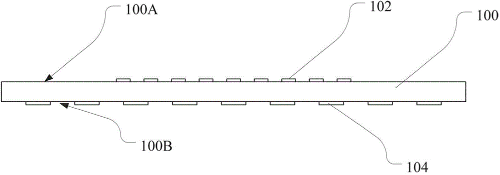
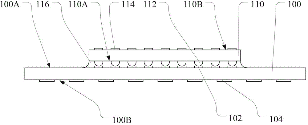
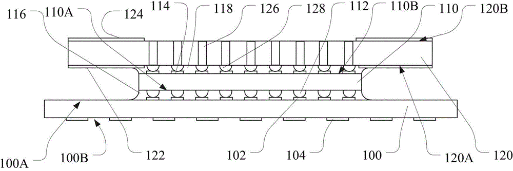
[0040] Please refer to Figure 1 to Figure 4 , Figure 1 to Figure 4 A schematic cross-sectional view showing various steps of a method for manufacturing a flip-chip stack package according to an embodiment of the present invention. The manufacturing method of the flip-chip stacked package of the present invention comprises the following steps: first please refer to figure 1, providing a packaging substrate 100, the packaging substrate 100 has an inner surface 100A and a corresponding ...


PUM


Abstract

The present invention provides the flip chip stacked package, an intermediary layer is applied to the flip chip stacked package to connect a first chip and a second chip, and comprises a first jointing surface and a corresponding second jointing surface; a plurality of conductive penetrating holes penetrating the first and second jointing surfaces; a first radiating metal layer configured on the first jointing surface; a second radiating metal layer configured on the second jointing surface, wherein the first and second radiating metal layers are in electrical isolation with the conductive penetrating holes, and between the adjacent conductive penetrating holes, the first radiating metal layer is arranged on the first jointing surface, and the second radiating metal layer is arranged on the second jointing surface. The first chip is configured on the first jointing surface, the second chip is configured on the second jointing surface, and the first and second chips are connected electrically via the conductive penetrating holes.

Description

technical field [0001] The present invention relates to a stacked package, and in particular to a flip-chip stacked package that can improve heat dissipation. Background technique [0002] With the thinning and thinning of electronic products, the integration level of semiconductor chips and the demand for high-density semiconductor packaging also increase accordingly. Stacked chip semiconductor package (stacked chip package), system-in-package (system in package), can accommodate multiple chips in one package to increase packaging density, so it has been widely used in many electronic products in recent years. In the semiconductor packaging technology, the flip chip technology (flip chip) allows the contacts of the chip to be arranged in an array, and provides an excellent bonding method between the chip and the packaging substrate for a high-pin count chip. These highly integrated chips and high-density packaging structures will generate relatively more heat energy during...

Claims


Application Information

Patent Timeline
IPC IPC(8): H01L23/538H01L23/367H01L25/00
CPCH01L2224/16227H01L2224/16235H01L2224/17181H01L2224/32225H01L2224/32245H01L2224/33181H01L2224/73204H01L2224/73253H01L2224/81192H01L2225/06517H01L2225/06572H01L2225/06589H01L2924/15313H01L2924/16251H01L2224/16225H01L2924/00
Inventor 许翰诚
Owner CHIPMOS TECH INC
Features
  • R&D
  • Intellectual Property
  • Life Sciences
  • Materials
  • Tech Scout
  • Unparalleled Data Quality
  • Higher Quality Content
  • 60% Fewer Hallucinations
Learn More