Method for performing memory interface control of an electronic device, and associated apparatus

A storage interface, electronic device technology, applied in information storage, static memory, automatic power control, etc., can solve the problems of signal offset, difficult timing allocation, etc., to achieve the effect of ensuring overall performance

Inactive Publication Date: 2015-09-09
MEDIATEK INC
View PDF5 Cites 8 Cited by
  • Summary
  • Abstract
  • Description
  • Claims
  • Application Information

AI Technical Summary

Problems solved by technology

For example, lines of different lengths may cause signal skew issues
In particular, when the difference between the lengths of two lines reaches thousands of micrometers (micrometers), for example, it will be difficult to allocate timing

Method used


Image

  • Method for performing memory interface control of an electronic device, and associated apparatus
  • Method for performing memory interface control of an electronic device, and associated apparatus
  • Method for performing memory interface control of an electronic device, and associated apparatus

Examples


Embodiment Construction

[0024] Certain words are used both in the specification and in the claims to represent identified elements. Those skilled in the art can understand that different electronic equipment manufacturers may use different names for the same component. This application distinguishes elements by function, not by name. In addition, in the specification and claims, the word "comprising" is open-ended, and it should be understood as "including, but not limited to...". Likewise, the word "connected" should be understood as an indirect or direct electrical connection. Thus, if a device is connected to another device, that connection may be a direct electrical connection or an indirect electrical connection through connection of the other device.

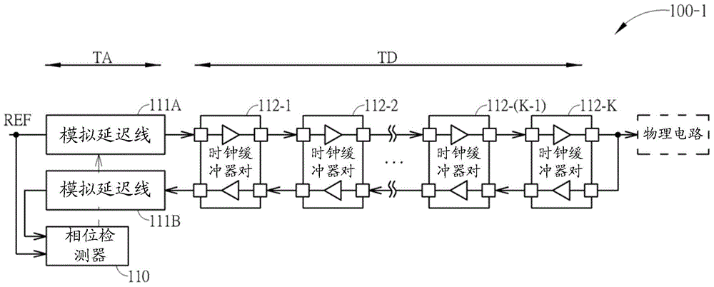
[0025] figure 1 It is a schematic diagram of a device 100-1 for performing storage interface control on an electronic device according to an embodiment of the present invention. See figure 1 , the device 100-1 includes at least a part (eg pa...


PUM


Abstract

A method for performing memory interface control of an electronic device and an associated apparatus are provided, where the method includes the steps of: when it is detected that a phase difference between a data signal and a clock signal reaches a predetermined value, controlling the clock signal to switch from a first frequency to a second frequency, wherein both of the clock signal and the data signal are signals of a memory interface circuit of the electronic device, and the memory interface circuit is arranged for controlling a random access memory (RAM) of the electronic device; applying at least one phase shift to the data signal until a condition is satisfied; and controlling the clock signal to switch from the second frequency to the first frequency; wherein the memory interface circuit is calibrated with aid of the at least one phase shift.

Description

technical field [0001] The present invention relates to a technology for timing control of signals between a system on chip (System on Chip, SoC) architecture and a memory chip, and more specifically, to a method and device for performing storage interface control on an electronic device. Background technique [0002] In the prior art, semiconductor chips can be integrated and packaged in the same package to reduce the size of the printed circuit board and / or the size of the electronic device. Taking the SOC architecture as an example, the semiconductor chip may include a SOC chip and a random access memory (Random Access Memory, hereinafter referred to as RAM) chip, wherein there are multiple storage interface terminals (memory interface terminals) near the four sides of the SOC chip. , and a plurality of storage interface terminals are arranged near the four sides of the RAM chip. In the prior art, the RAM chip can be disposed on the SOC chip, and the storage interface te...

Claims


Application Information

Patent Timeline
Patent Type & Authority Applications(China)
IPC IPC(8): G06F13/16
CPCG11C7/1072G06F13/1673G11C7/1066G11C7/1093G11C7/222H03L7/0816H03L7/0818H03L7/0994H03L2207/50G06F1/04G06F1/08G06F1/10G06F1/12
Inventor 陈尚斌谢博伟
Owner MEDIATEK INC
Why Eureka
Try Eureka