Semiconductor device, method of manufacturing semiconductor device, and electronic apparatus
A semiconductor and atomic technology, used in semiconductor/solid-state device manufacturing, semiconductor devices, radiation control devices, etc., can solve problems such as the increase in the size of semiconductor substrates, the difficulty in controlling the residual hydrogen content of passivation films, and the inability to configure active components. , to achieve the effect of suppressing the increase in size
Active Publication Date: 2015-09-09
SONY CORP
View PDF6 Cites 1 Cited by
- Summary
- Abstract
- Description
- Claims
- Application Information
AI Technical Summary
Problems solved by technology
[0010] However, according to the method of Japanese Patent Application Laid-Open No. 2009-188068, it is difficult to control the remaining hydrogen amount of the passivation film in a region not far from the boundary between the pixel portion and the peripheral circuit portion
Therefore, active elements, etc., whose hydrogen supply amount is ideally controlled cannot be arranged, which leads to an increase in the size of the semiconductor substrate
Method used
View moreImage
Smart ImageViewing Examples

Examples
no. 1 approach
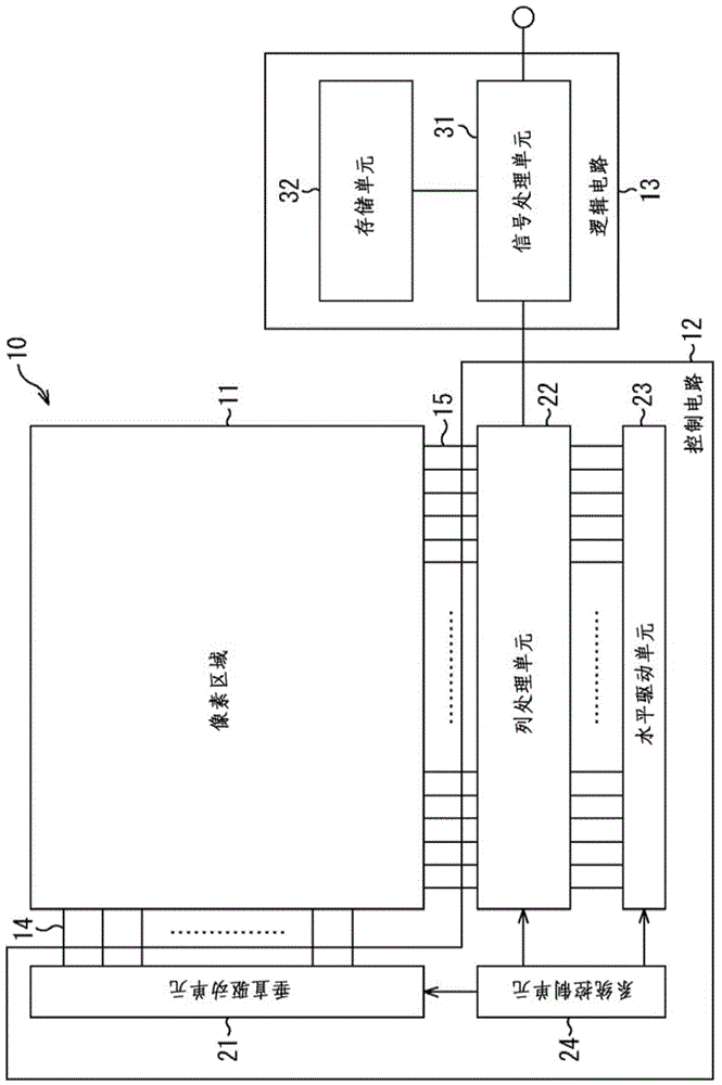
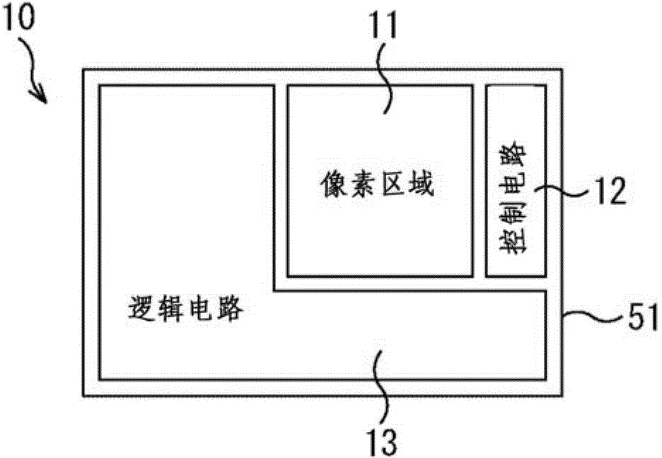
[0066] 1. First embodiment: CMOS image sensor ( Figure 1-13 )
no. 2 approach
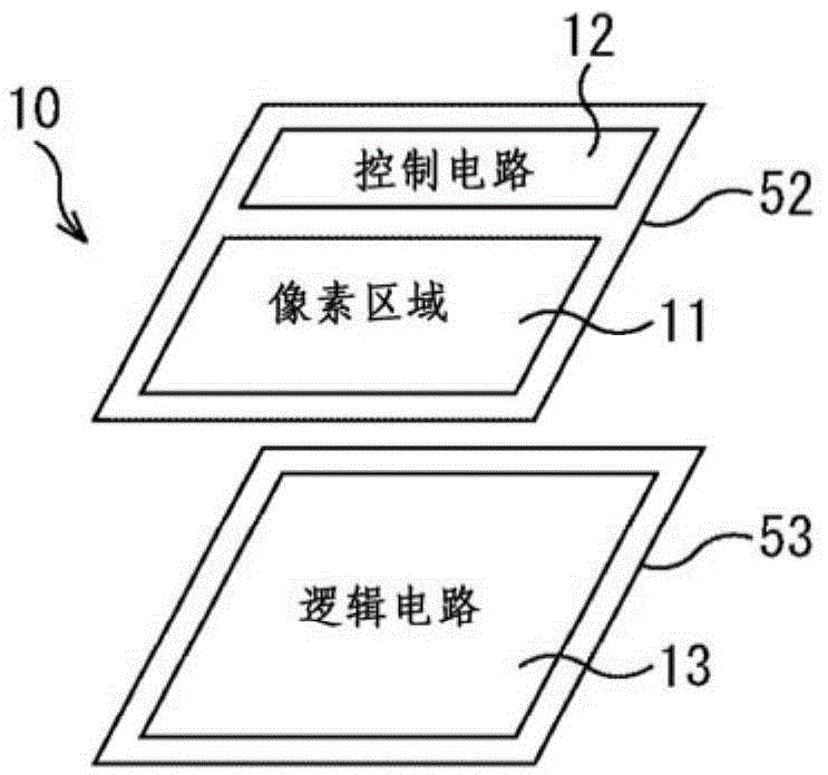
[0067] 2. The second embodiment: CMOS image sensor ( Figures 14-28 )
no. 3 approach
[0068] 3. The third embodiment: CMOS image sensor ( Figures 29 to 32 )
Login to View More PUM
 Abstract
Disclosed is a semiconductor device including a first semiconductor substrate and a first atom diffusion prevention portion, the first atom diffusion prevention portion being arranged at a part on the first semiconductor substrate and configured to prevent diffusion of an atom having a dangling bond terminating effect.
Description
[0001] Cross References to Related Applications [0002] This application claims the benefit of Japanese Priority Patent Application JP2014-040388 filed on Mar. 3, 2014, the entire contents of which are incorporated herein by reference. technical field [0003] The present disclosure relates to a semiconductor device, a method of manufacturing the semiconductor device, and an electronic device, and in particular, to a method capable of suppressing the size of a semiconductor substrate while controlling the concentration of atoms having a dangling bond termination effect on the surface of the semiconductor substrate for each region. An enlarged semiconductor device, a method of manufacturing the semiconductor device, and an electronic device. Background technique [0004] In a solid-state image pickup element such as a CCD (Charge Coupled Device) or a CMOS (Complementary Metal Oxide Semiconductor) image sensor, it is important to reduce dark current on the surface of a semico...
Claims
Login to View More Application Information
Patent Timeline
 IPC IPC(8): H01L27/146H04N5/335
CPCH01L27/14689H01L27/14643H01L27/1463H01L27/1469H01L27/14634H01L27/14614H01L27/1462H01L27/14636H01L21/76897H01L27/14603H01L27/14612H01L27/1464
Inventor 马场公一场色正昭江尻洋一
Owner SONY CORP