Optical detector based on BiCuSeO thermoelectric thin-film transverse thermoelectric effect
A lateral thermoelectric, bismuth copper selenide technology, applied in the direction of thermoelectric device node lead-out material, electric solid device, circuit, etc., can solve the problems of wide response band, high detection sensitivity, low detection sensitivity, etc., to achieve wide response band , the effect of high detection sensitivity
- Summary
- Abstract
- Description
- Claims
- Application Information
AI Technical Summary
Problems solved by technology
Method used
Image
Examples
Example Embodiment
[0026] Example 1
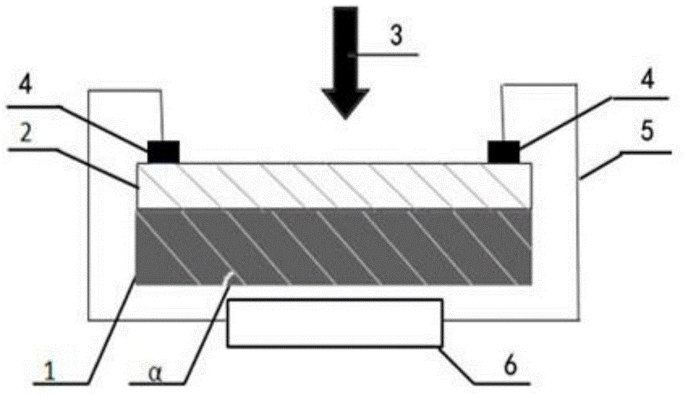
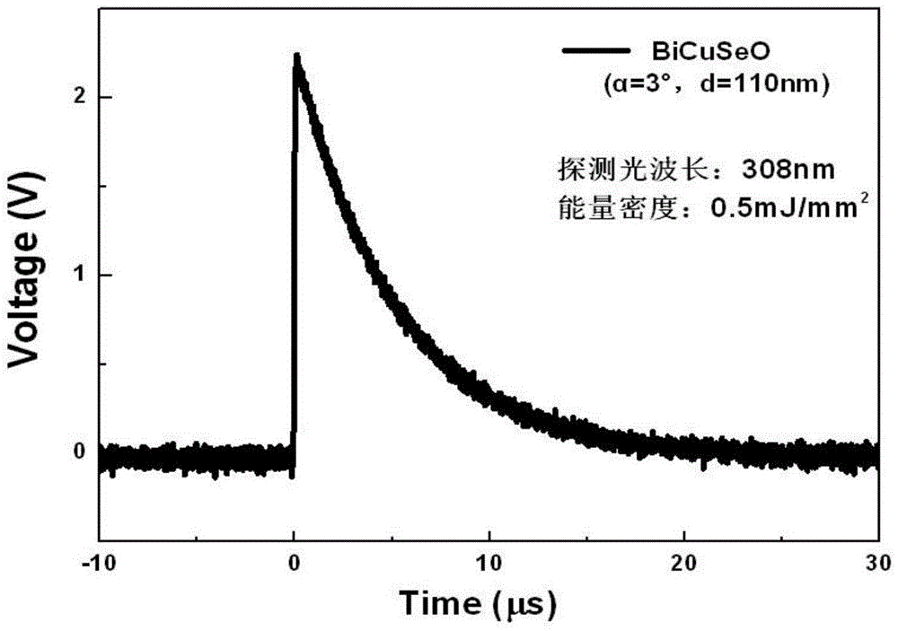
[0027] 1. The transverse thermoelectric element adopts LaAlO obliquely cut at 3° on the c axis 3 A layer of bismuth-copper-selenium-oxygen thin film with a thickness of 110nm grown obliquely along the c-axis was prepared on a single crystal substrate with a tilt angle of 3°.
[0028] The specific preparation process is as follows: Weigh Bi according to the atomic molar ratio of the chemical formula BiCuSeO 2 O 3 , Elemental Cu, Bi and Se are mixed to obtain a mixture material, the mixture material is ground in a ball mill for 30 hours, the ground material is pressed into a disc with a thickness of 3mm and a diameter of 25mm, and the above disc is vacuum sealed Technology The wafer is encapsulated in a quartz tube and then sintered by a high-temperature solid-phase reaction method to obtain the required bismuth copper selenium oxide polycrystalline ceramic target. Put the obtained bismuth-copper-selenium-oxygen polycrystalline ceramic target into the PLD cavity, a...
Example Embodiment
[0034] Example 2
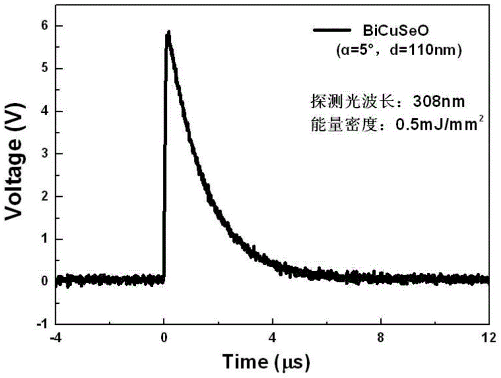
[0035] 1. The transverse thermoelectric element adopts LaAlO which is obliquely cut at 5° on the c axis 3 A layer of bismuth-copper-selenium-oxygen thin film with a thickness of 110nm and grown obliquely along the c-axis was prepared on a single crystal substrate with a tilt angle of 5°.
[0036] The specific preparation process is as follows: Weigh Bi according to the atomic molar ratio of the chemical formula BiCuSeO 2 O 3 , Elemental Cu, Bi and Se are mixed to obtain a mixture material, the mixture material is ground in a ball mill for 30 hours, the ground material is pressed into a disc with a thickness of 3mm and a diameter of 25mm, and the above disc is vacuum sealed Technology The wafer is encapsulated in a quartz tube and then sintered by a high-temperature solid-phase reaction method to obtain the required bismuth copper selenium oxide polycrystalline ceramic target. Put the obtained bismuth-copper-selenium-oxygen polycrystalline ceramic target into the ...
Example Embodiment
[0042] Example 3
[0043] 1. The transverse thermoelectric element adopts LaAlO which is obliquely cut 10° on the c axis 3 A layer of bismuth-copper-selenium-oxygen thin film with a thickness of 110nm and grown obliquely along the c-axis was prepared on a single crystal substrate with a tilt angle of 10°.
[0044] The specific preparation process is as follows: Weigh Bi according to the atomic molar ratio of the chemical formula BiCuSeO 2 O 3 , Elemental Cu, Bi and Se are mixed to obtain a mixture material, the mixture material is ground in a ball mill for 30 hours, the ground material is pressed into a disc with a thickness of 3mm and a diameter of 25mm, and the above disc is vacuum sealed Technology The wafer is encapsulated in a quartz tube and then sintered by a high-temperature solid-phase reaction method to obtain the required bismuth copper selenium oxide polycrystalline ceramic target. Put the obtained bismuth-copper-selenium-oxygen polycrystalline ceramic target into the P...
PUM
| Property | Measurement | Unit |
|---|---|---|
| Thickness | aaaaa | aaaaa |
| Thickness | aaaaa | aaaaa |
| Diameter | aaaaa | aaaaa |
Abstract
Description
Claims
Application Information


