A stepped groove circuit board and its processing method

A processing method and step groove technology, applied in printed circuit, printed circuit manufacturing, printed circuit parts, etc., to achieve the effect of not being easily polluted

Active Publication Date: 2018-08-07
SHENNAN CIRCUITS
View PDF5 Cites 0 Cited by
  • Summary
  • Abstract
  • Description
  • Claims
  • Application Information

AI Technical Summary

Problems solved by technology

[0008] The embodiment of the present invention provides a stepped groove circuit board and its processing method to solve the above-mentioned various problems existing in the prior art when manufacturing a stepped groove circuit board with metallized through holes in the stepped groove area.

Method used


Image

  • A stepped groove circuit board and its processing method
  • A stepped groove circuit board and its processing method
  • A stepped groove circuit board and its processing method

Examples


Embodiment 1

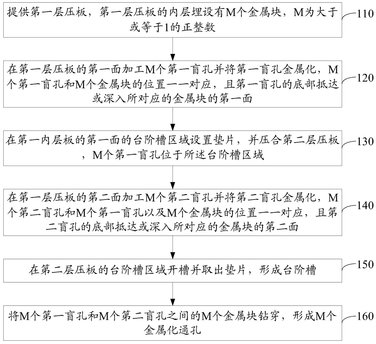
[0038] Please refer to figure 1 , an embodiment of the present invention provides a method for processing a stepped groove circuit board, which may include:

[0039] 110. Provide a first laminate, where M metal blocks are embedded in the inner layer of the first laminate, where M is a positive integer greater than or equal to 1.

[0040] Assume that a multilayer circuit board of (P+Q) layer needs to be made in the end, wherein P and Q are both positive integers greater than or equal to 1; and step grooves need to be processed on the multilayer circuit board, assuming Located on the (P+1)th floor to (P+Q)th floor.

[0041] In this step, the first laminate is prefabricated, and the first laminate includes the first layer to the Pth layer. Assuming that the bottom of the stepped groove of the stepped groove circuit board is designed with M metallized through holes, the M metalized through holes need to be located in the stepped groove area of ​​the first laminate and run throug...


PUM


Abstract

The invention discloses a step-groove circuit board and a processing method thereof so as to solve various problems existing when producing the step-groove circuit board, where metalized through holes are designed in a step-groove area in the prior art. The method comprises the following steps: processing a first surface of a first laminated board to form first blind holes and metalizing the blind holes, the bottom portion of each of the first blind holes reaching or penetrating into a first surface of a metal block in the first laminated board; arranging a pad in the step-groove area of the first surface of the first inner-layer board and laminating a second laminated board; processing a second surface of the first laminated board to form M second blind holes and metalizing the blind holes, the positions of the M second blind holes being in one-to-one correspondence with the positions of the M first blind holes and positions of the M metal blocks respectively, and the bottom portion of each second blind hole reaching or penetrating into a second surface of the corresponding metal block; carrying out slotting on the step-groove area of the second laminated board and taking the pad out to form a step groove; and drilling the M metal blocks between the M first blind holes and the M second blind holes to form M metalized through holes.

Description

technical field [0001] The invention relates to the technical field of circuit boards, in particular to a stepped groove circuit board and a processing method thereof. Background technique [0002] At present, there are more and more applications of step groove circuit boards. There is such a special design, that is, there is a metallized through hole under the step groove, which is used as a plug hole or a conduction hole or a heat dissipation hole, and the metallization Via holes are not allowed to be plugged. [0003] The manufacturing method of the step groove circuit board with metallized through holes designed in the step groove area includes the following steps: non-step level lamination, drilling at the position of the step groove, sinking copper electroplating, attaching gaskets, step level lamination, Immersion copper electroplating, outer layer graphic production, step slotting, desmearing, surface production, etc. [0004] But there is following defect in above...

Claims


Application Information

Patent Timeline
Patent Type & Authority Patents(China)
IPC IPC(8): H05K1/11H05K1/02H05K3/00H05K3/42
Inventor 刘宝林
Owner SHENNAN CIRCUITS
Why Eureka
Try Eureka