Semiconductor laser light source
A laser light source, semiconductor technology, applied in the direction of semiconductor lasers, lasers, structures of optical waveguide semiconductors, etc.
- Summary
- Abstract
- Description
- Claims
- Application Information
AI Technical Summary
Problems solved by technology
Method used
Image

Examples
Embodiment approach 1
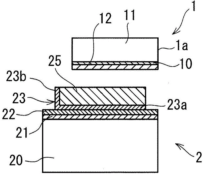
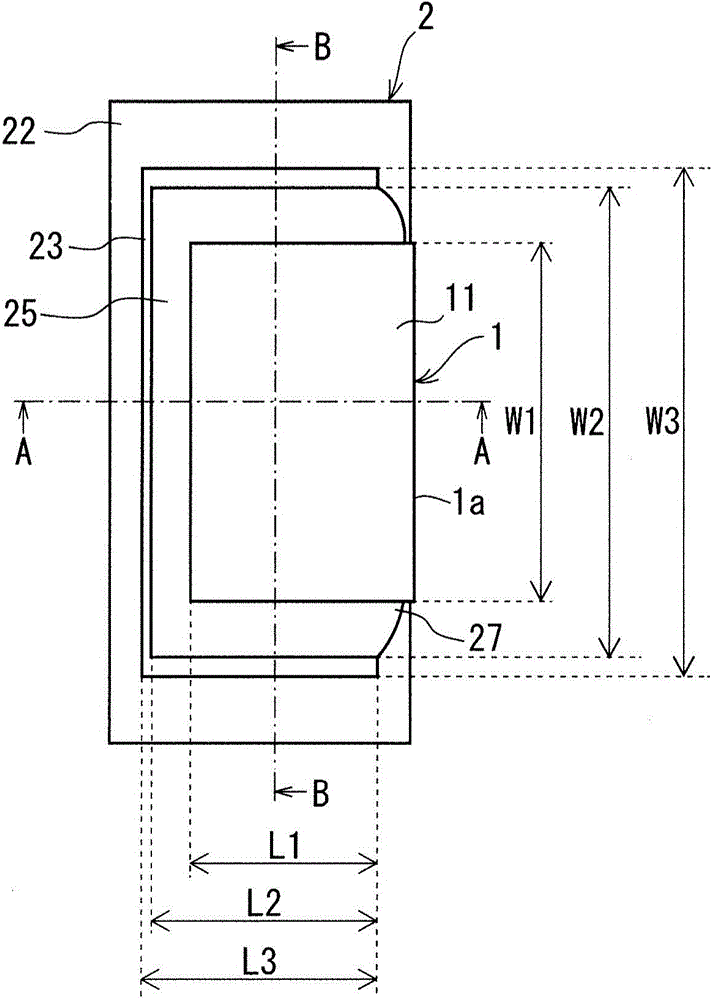
[0031] Embodiment 1 of the present invention will be described below using the drawings. figure 1 It is a cross-sectional view showing the state before the semiconductor laser 1 and the base 2 are joined in the semiconductor laser light source of Embodiment 1, figure 2 It is a plan view of the semiconductor laser light source of Embodiment 1, image 3 yes figure 2 The A-A line sectional view, Figure 4 yes figure 2 B-B line sectional view.
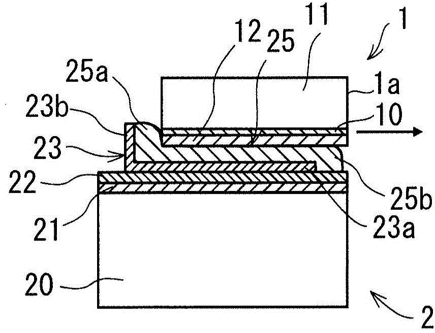
[0032] Such as figure 1 As shown, the semiconductor laser light source includes a semiconductor laser 1 and a base 2 . The semiconductor laser 1 has, for example, a multi-emitter structure in which a plurality of light-emitting points exist. The semiconductor laser 1 includes a semiconductor laser substrate 11 , an active layer 10 and an Au layer 12 .
[0033] The active layer 10 is disposed on the semiconductor laser substrate 11 figure 1 in the lower surface. Since the output characteristics and reliability of the semiconduct...
Embodiment approach 2
[0053] Next, a semiconductor laser light source according to Embodiment 2 will be described. Figure 6 is a cross-sectional view showing the state before the semiconductor laser 1 is joined to the base 32 in the semiconductor laser light source of Embodiment 2, Figure 7 It is a sectional view of the semiconductor laser light source of Embodiment 2. It should be noted that, in Embodiment 2, the same components as those described in Embodiment 1 are assigned the same reference numerals to omit description.
[0054] Such as Figure 6 and Figure 7 As shown, in Embodiment 2, the Au film 31 is arranged on the side surface of the base 32 corresponding to the output terminal 1 a side of the semiconductor laser 1 . It should be noted that other structures of the base 32 are the same as those of the base 2 .
[0055] As described above, in the semiconductor laser light source according to Embodiment 2, since the Au film 31 is disposed on the side surface of the base 32 correspondi...
Embodiment approach 3
[0057] Next, a semiconductor laser light source according to Embodiment 3 will be described. Figure 8 is a cross-sectional view showing the state before the semiconductor laser 1 is joined to the base 42 in the semiconductor laser light source of Embodiment 3, Figure 9 It is a plan view of the semiconductor laser light source of Embodiment 3, Figure 10 yes Figure 9 C-C line sectional view. In Embodiment 3, the same components as those described in Embodiments 1 and 2 are denoted by the same reference numerals to omit description.
[0058] Such as Figure 8 to Figure 10 As shown, in the third embodiment, the structure of the barrier layer 23 of the base 42 is different from that in the first and second embodiments. The barrier portion 23b of the barrier layer 23 is formed over the entire outer circumference of the outer peripheral portion of the horizontal portion 23a. That is, the blocking portion 23b is formed over the entire outer peripheral portion corresponding to...
PUM
 Abstract
Description
Claims
Application Information
 - R&D
- Intellectual Property
- Life Sciences
- Materials
- Tech Scout
- Unparalleled Data Quality
- Higher Quality Content
- 60% Fewer Hallucinations
Browse by: Latest US Patents, China's latest patents, Technical Efficacy Thesaurus, Application Domain, Technology Topic, Popular Technical Reports.
© 2025 PatSnap. All rights reserved.Legal|Privacy policy|Modern Slavery Act Transparency Statement|Sitemap|About US| Contact US: help@patsnap.com