Module and method for producing same

A manufacturing method and molding resin technology, applied in semiconductor/solid-state device manufacturing, semiconductor/solid-state device components, semiconductor devices, etc., can solve problems such as difficulty in ensuring module connection reliability, and achieve the effect of preventing poor connection

Inactive Publication Date: 2015-09-16
MURATA MFG CO LTD
View PDF11 Cites 8 Cited by
  • Summary
  • Abstract
  • Description
  • Claims
  • Application Information

AI Technical Summary

Problems solved by technology

[0003] However, since the flip-chip mounting method is to form bumps made of solder, Au, etc., on electrodes on the circuit formation surface of an IC, which is an electronic component, for example, and use the bumps to directly connect the IC to the wiring substrate, Therefore, the stress generated between the wiring board and electronic components tends to concentrate on the connection part, making it difficult to ensure the connection reliability of the module

Method used


Image

  • Module and method for producing same
  • Module and method for producing same
  • Module and method for producing same

Examples


Embodiment approach 1

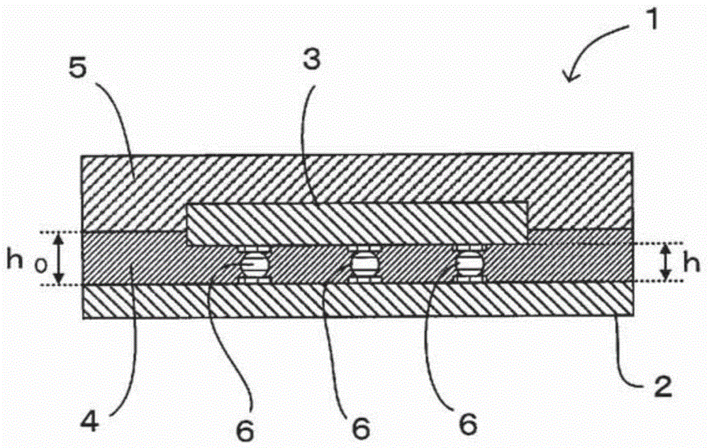
[0039] refer to figure 1 The module 1 according to Embodiment 1 of the present invention will be described. figure 1 It is a sectional view of the module 1 of Embodiment 1.

[0040] The module 1 of this embodiment is as figure 1 As shown, it includes: a wiring substrate 2; electronic components 3 mounted on one main surface of the wiring substrate 2; formed on the entire surface of one main surface of the wiring substrate 2, and connecting one main surface of the wiring substrate 2 with the electronic components an underfill resin layer 4 filling the gaps between the devices 3 ; and a molding resin layer 5 formed to cover the electronic components 3 and the underfill resin layer 4 .

[0041] The wiring substrate 2 is made of, for example, a glass epoxy substrate, a low temperature co-fired ceramic (LTCC) substrate, a glass substrate, etc., and wiring electrodes and / or via conductors are formed on its main surface and / or inside. In addition, any one of a multilayer substr...

Embodiment approach 2

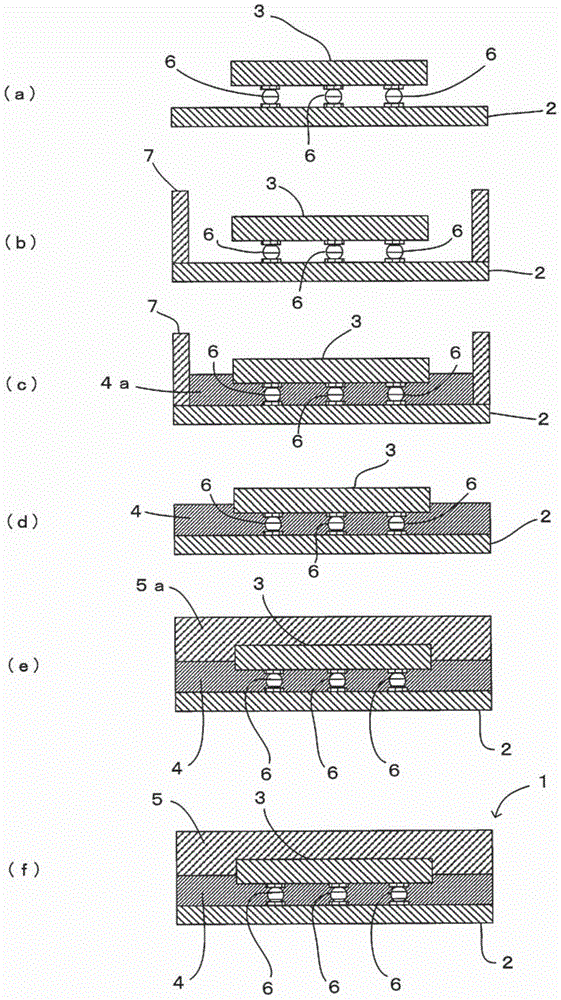
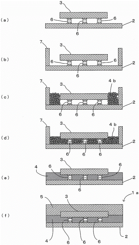
[0064] refer to image 3 The module 1a according to Embodiment 2 of the present invention will be described. in addition, image 3 It is a figure for demonstrating the manufacturing method of the module 1a of Embodiment 2, image 3 (a)~ image 3 (f) shows each process.

[0065] Module 1a of this embodiment and reference figure 1 and figure 2 The module 1 of Embodiment 1 described above is different in that the underfill resin layer 4 is formed using the powdered resin 4 b in the manufacturing method. The other configurations are the same as those of the module 1 in Embodiment 1, and thus the description of the configurations will be omitted by denoting the same configurations with the same reference numerals.

[0066] in addition, image 3 In each process of the manufacturing method of the module 1a shown, image 3 The steps shown in (a) to (b) correspond to figure 2 The steps shown in (a) to (b), image 3 The process shown in (f) corresponds to figure 2 (e), si...

Embodiment approach 3

[0075] refer to Figure 4 Module 1b according to Embodiment 3 of the present invention will be described. in addition, Figure 4 is a cross-sectional view of module 1b.

[0076] Module 1b of this embodiment and reference figure 1 The differences of the module 1 of the first embodiment described are as follows: Figure 4 As shown, the molding resin layer 5 has a double-layer structure. The other configurations are the same as those of the module 1 in Embodiment 1, and thus the description of the configurations will be omitted by denoting the same configurations with the same reference numerals.

[0077] In this case, the molded resin layer 5 is composed of the first molded resin layer 5b disposed adjacent to the upper side of the underfill resin layer 4 and the second molded resin layer disposed above the first molded resin layer 5b. The resin layer 5c is formed. In addition, the particle diameter of the filler contained in the first molded resin layer 5b and the particl...


PUM


Abstract

The purpose of the present invention is to provide a module which is capable of improving the connection reliability between a wiring board and an electronic component that is mounted on the wiring board. A module (1) is provided with: a wiring board (2); an electronic component (3) that is mounted on one main surface of the wiring board (2); an underfill resin layer (4) that is formed on all over the surface of the one main surface of the wiring board (2) so as to fill up the gap between the one main surface of the wiring board (2) and the electronic component (3); and a mold resin layer (5) that is formed so as to cover the underfill resin layer (4) and the electronic component (3). The underfill resin layer (4) is formed of a resin which contains a filler having a particle diameter that is smaller than the distance between the one main surface of the wiring board (2) and the electronic component (3).

Description

technical field [0001] The present invention relates to a module in which electronic components mounted on a wiring board are covered with a resin layer and a method for manufacturing the same. Background technique [0002] In recent years, a flip chip mounting method has been widely used as a method of mounting electronic components on the surface of a wiring board in a module including a wiring board and electronic components. Compared with the method of mounting electronic components by wire bonding, this mounting method can reduce the mounting area of ​​the electronic components, and thus can realize miniaturization of the module. In addition, since the wiring length for connecting the electronic components and the wiring board can be shortened, the electrical characteristics of the module can be improved. [0003] However, since the flip-chip mounting method is a method in which bumps made of solder, Au, etc. are formed on electrodes of, for example, the circuit format...

Claims


Application Information

Patent Timeline
Patent Type & Authority Applications(China)
IPC IPC(8): H01L23/29H01L21/56H01L21/60H01L23/31H01L25/00
CPCH01L21/563H01L23/3121H01L24/13H01L2224/92125H01L2224/32225H01L24/32H01L2224/73204H01L25/16H01L2224/16225H01L2924/19105H01L2224/83001H01L24/16H01L23/29H01L2224/81815H01L2924/10253H01L2224/48091H01L2924/10329H01L24/73H01L21/565H01L24/81H01L2224/81H01L2224/45144H01L2224/13101H01L23/3737H01L23/3135H01L24/29H01L24/83H01L24/92H01L2224/2929H01L2224/29386H01L2224/29387H01L2224/29393H01L2924/15787H01L2924/15788H01L2924/1579H01L2924/19041H01L2924/19042H01L2924/19043H01L23/295H01L2924/00014H01L2924/00012H01L2924/00015H01L2924/014H01L23/3114H01L23/49838H01L21/4803H01L23/49894H01L25/0655H01L2924/0665H01L2924/066H01L2924/07025H01L2924/06H01L2924/05442H01L2924/05432H01L2924/05032H01L2924/05042H01L2924/01006
Inventor 伊藤悟志
Owner MURATA MFG CO LTD
Why Eureka
Try Eureka