
Array substrate, manufacture method thereof, and display device

A technology of an array substrate and a manufacturing method, applied in the display field, can solve the problems of prone to faults, pixel electrodes 7 providing data signals, reducing the yield of array substrate products, etc., so as to ensure display effect, improve product yield, and optimize connection conditions Effect

Inactive Publication Date: 2015-09-23
BOE TECH GRP CO LTD +1
View PDF3 Cites 6 Cited by
  • Summary
  • Abstract
  • Description
  • Claims
  • Application Information

AI Technical Summary

Problems solved by technology

[0004] In the traditional HADS array substrate, the positions of the common electrode and the pixel electrode of the ADS array substrate are reversed. The process flow of the HADS array substrate is: forming gate electrode 2 and gate line → forming active layer 4 → forming source electrode 5 and drain electrode 6. Data line and pixel electrode 7 → form a common electrode, such as figure 1 and figure 2 As shown, the pixel electrode 7 and the drain electrode 6 are arranged on the same layer, and the pixel electrode 7 is directly overlapped on the drain electrode 6. However, since the thickness of the pixel electrode 7 is generally relatively thin, faults are likely to occur at the overlapping slope angle, resulting in The drain electrode 6 and the pixel electrode 7 are disconnected, so that the drain electrode 6 cannot provide data signals for the pixel electrode 7, thereby affecting the normal operation of the array substrate and reducing the product yield of the array substrate

Method used


Image

  • Array substrate, manufacture method thereof, and display device
  • Array substrate, manufacture method thereof, and display device
  • Array substrate, manufacture method thereof, and display device

Examples


Embodiment 1

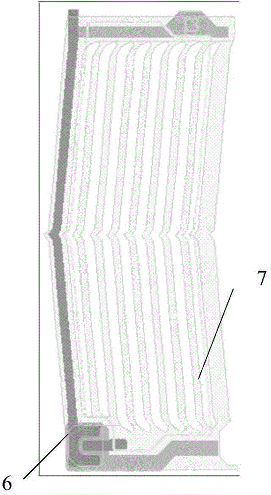
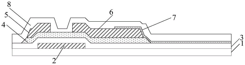
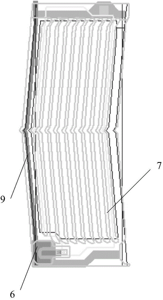
[0052] This embodiment provides an array substrate, including a plurality of pixel areas, each pixel area includes:

[0053] The pixel electrode and the drain electrode are arranged in the same layer and are independent of each other, and the pixel electrode and the drain electrode are connected through conductive components of different layers;

[0054] Wherein, an insulating layer is separated between the pixel electrode, the drain electrode, and the conductive member, and a position corresponding to the drain electrode of the insulating layer has a first via hole penetrating through the insulating layer, and the insulating layer is connected to the insulating layer. The position corresponding to the pixel electrode has a second via hole through the insulating layer, the drain electrode is connected to the conductive component through the first via hole, and the pixel electrode is connected to the conductive component through the second via hole. The above-mentioned conducti...

Embodiment 2

[0065] This embodiment provides a display device, including the above array substrate. The display device can be any product or component with a display function such as a liquid crystal panel, a liquid crystal TV, a liquid crystal display, a digital photo frame, a mobile phone, and a tablet computer.

Embodiment 3

[0067] This embodiment provides a method for manufacturing an array substrate, the array substrate includes a plurality of pixel regions, and the method includes:

[0068] In each pixel region, a pixel electrode and a drain electrode arranged in the same layer and independent of each other are formed, and a conductive member of a different layer is formed to connect the pixel electrode and the drain electrode;

[0069] Wherein, an insulating layer is separated between the pixel electrode, the drain electrode, and the conductive member, and a position corresponding to the drain electrode of the insulating layer has a first via hole penetrating through the insulating layer, and the insulating layer is connected to the insulating layer. The position corresponding to the pixel electrode has a second via hole through the insulating layer, the drain electrode is connected to the conductive component through the first via hole, and the pixel electrode is connected to the conductive co...


PUM


Abstract

The invention provides an array substrate, a manufacture method thereof, and a display device, belonging to the display technical field. The array substrate comprises a plurality of pixel areas; each pixel area comprises a pixel electrode and a drain electrode which are arranged on a same layer and mutually independent; the pixel electrode and the drain electrode are in connection through a conductive component on a different layer; an insulating layer is arranged among the pixel electrode, the drain electrode and the conductive component; the insulating layer is provided with a first via hole penetrating the insulating layer at a position corresponding with the drain electrode, and is provided with a second via hole penetrating the insulating layer at a position corresponding with the pixel electrode; the drain electrode is in connection with the conductive component through the first via hole; the pixel electrode is in connection with the conductive component through the second via hole. The technical scheme of the invention can optimize the connection between the pixel electrode and the drain electrode, and increase the product yield rate of the array substrate.

Description

technical field [0001] The present invention relates to the field of display technology, in particular to an array substrate, a manufacturing method thereof, and a display device. Background technique [0002] Liquid crystal display (LCD, Liquid Crystal Display) has the characteristics of small size, light weight, low power consumption, low radiation and low manufacturing cost, and has been widely used in various electronic devices, such as monitors, TVs, mobile phones, digital cameras, etc. digital electronics. Among them, TFT-LCD (Thin Film Transistor Liquid Crystal Display, Thin Film Transistor Liquid Crystal Display) is a main flat panel display device (FPD, Flat Panel Display). [0003] According to the direction of the electric field driving the liquid crystal, TFT-LCD is divided into vertical electric field type, horizontal electric field type and multi-dimensional electric field type. Among them, the vertical electric field type TFT-LCD needs to form pixel electrod...

Claims


Application Information

Patent Timeline
IPC IPC(8): H01L27/12H01L29/417H01L21/28
CPCG02F1/136227H01L27/124H01L27/1248H01L21/28G02F1/13439G02F1/1368H01L21/76804H01L27/1288H01L29/41733
Inventor 冯博苗青马禹
Owner BOE TECH GRP CO LTD
Features
  • Generate Ideas
  • Intellectual Property
  • Life Sciences
  • Materials
  • Tech Scout
  • Unparalleled Data Quality
  • Higher Quality Content
  • 60% Fewer Hallucinations
Learn More