TFT substrate group and manufacturing method therefor

A manufacturing method and a technology of a substrate group, which are applied in semiconductor/solid-state device manufacturing, electrical components, and electrical solid-state devices, etc., can solve problems such as increased consumption of etching solution, increased cost of copper manufacturing process, and incomplete etching, so as to reduce incomplete etching. The risk of exhaustion, the improvement of etching, and the effect of improving product quality

Active Publication Date: 2015-09-23
TCL CHINA STAR OPTOELECTRONICS TECH CO LTD
View PDF4 Cites 6 Cited by
  • Summary
  • Abstract
  • Description
  • Claims
  • Application Information

AI Technical Summary

Problems solved by technology

[0007] During the etching process of the copper process, as the concentration of copper ions in the etching solution increases, the etching ability of the etching solution decreases. Under different etching modes, there is a maximum concentration of copper ions. If this concentration is exceeded, there is a risk of unclean etching.
For example, in a certain etching mode, if the maximum concentration of copper ions in the etching solution is greater than 3000ppm, there will be a risk of incomplete etching; in addition, the copper process etching solution has a short service life of only 24 hours. These characteristics make the etching solution The life cycle is shortened and the cost of the copper process is increased
[0008] like figure 1 As shown, it is a schematic diagram of the design of the metal layer in an existing TFT substrate group; the TFT substrate group includes several TFT substrates 200 arranged in a matrix, and the passage between the several TFT substrates 200 is in the form of a grid. The interval regions 300 are spaced apart, and the metal electrodes 210 are respectively provided on the several TFT substrates 200. The interval regions 300 are not covered by the metal layer. The manufacturing method of the metal layer in the existing TFT substrate group is: in the TFT Metal copper is deposited on the surface of the substrate group to form a copper layer, and then the copper layer is patterned. In the process of patterning the copper layer, it is necessary to etch away all the copper located in the spacer region 300, and the etching of this part of the copper will Increase the concentration of copper ions in the etchant, thereby increasing the consumption of the etchant; and because the spacer region 300 often occupies a certain area ratio on the entire TFT substrate group, resulting in a low etching rate (Etching Rate), making this region prone to Incomplete etching phenomenon, such as Figure 2-3 As shown, metal copper remains in the space area 300 close to the metal electrode 210, so that the pattern of the metal layer cannot be realized according to the design pattern, which affects the stability of the process and the quality of the product.

Method used


Image

  • TFT substrate group and manufacturing method therefor
  • TFT substrate group and manufacturing method therefor
  • TFT substrate group and manufacturing method therefor

Examples


Embodiment Construction

[0039] In order to further illustrate the technical means adopted by the present invention and its effects, the following describes in detail in conjunction with preferred embodiments of the present invention and accompanying drawings.

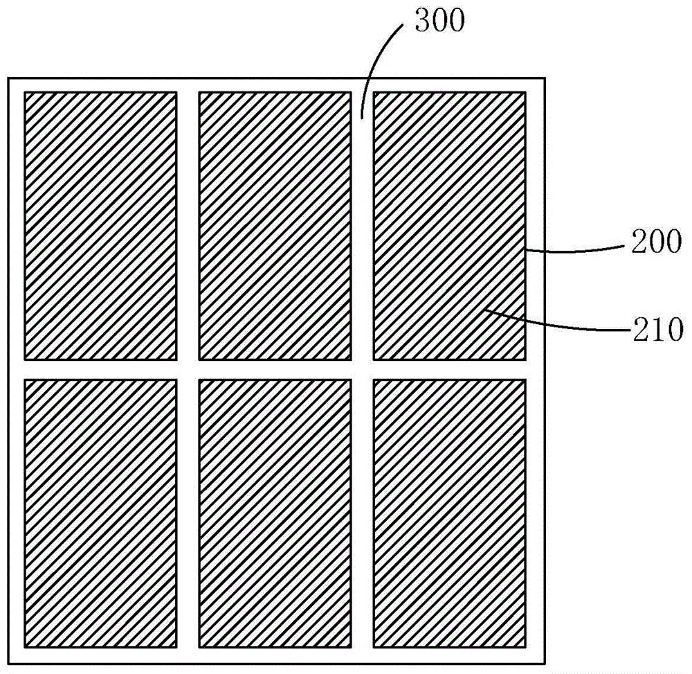
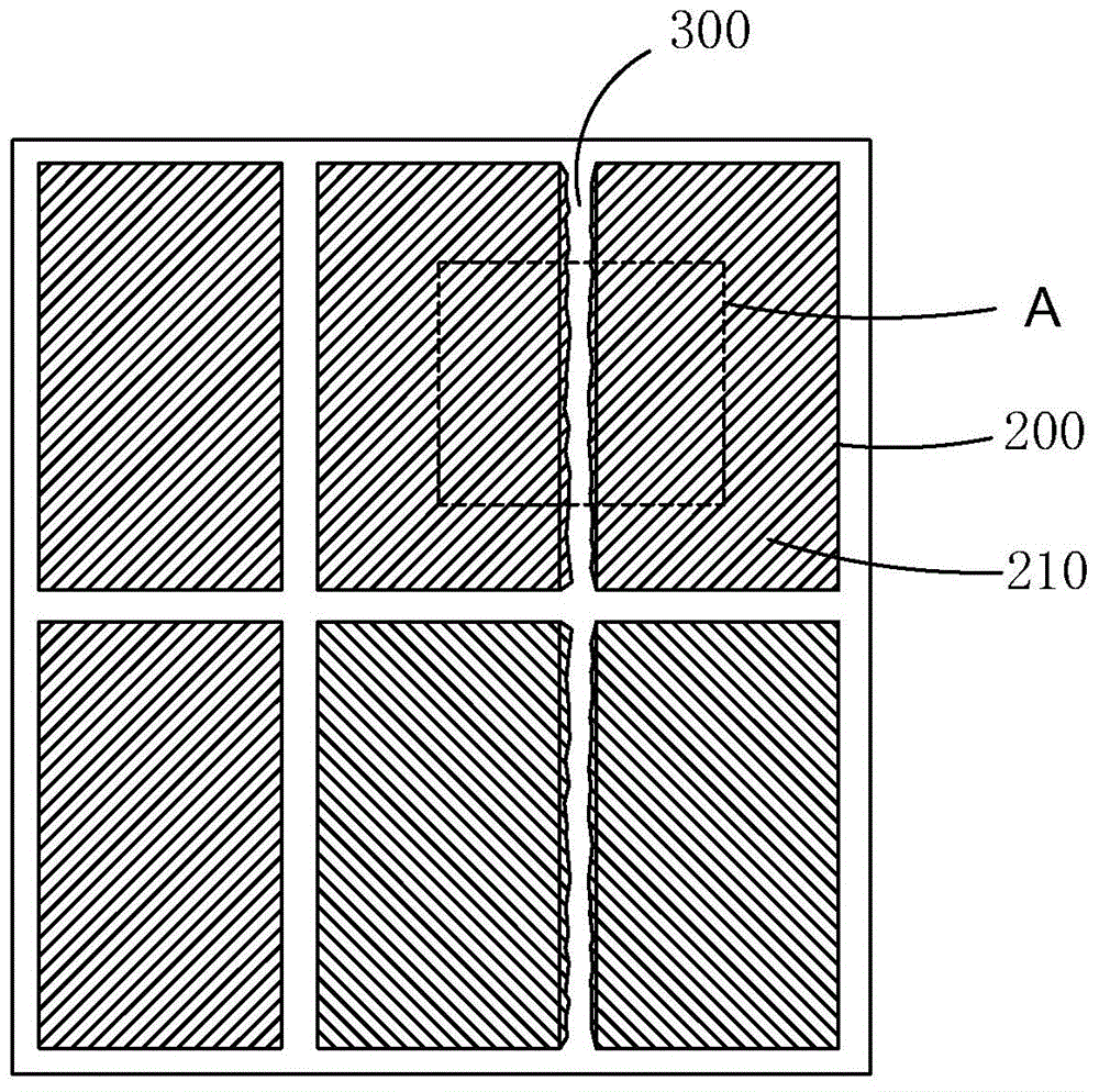
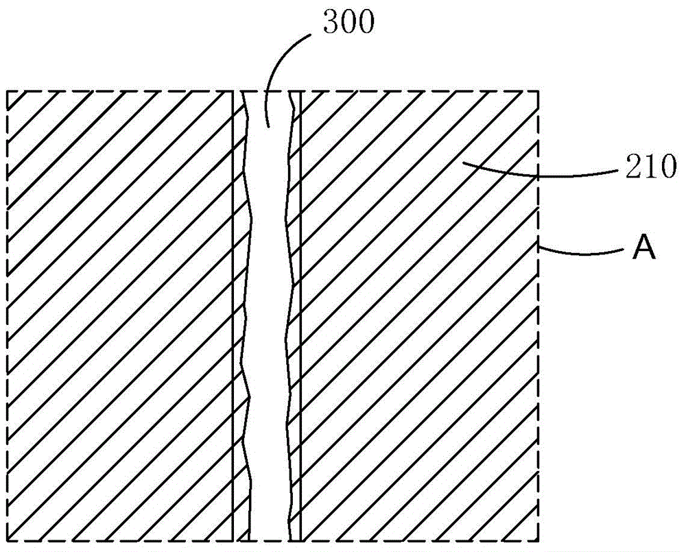
[0040] see Figure 4-5 , the present invention firstly provides a TFT substrate group, comprising: several TFT substrates 20, and a spacer area 30 between several TFT substrates 20 to separate the several TFT substrates 20, the TFT substrate 20 is provided with metal The electrode 21 is provided with a metal pattern 31 spaced from the metal electrode 21 in the spaced area 30 .

[0041] Specifically, the material of the metal electrode 21 and the metal pattern 31 is copper.

[0042] Wherein, the plurality of TFT substrates 20 are arranged in a matrix in the TFT substrate group.

[0043] The spacer regions 30 are distributed in grid form in the TFT substrate group.

[0044] Specifically, the shape of the metal electrode 21 is a rectangle.

[0...


PUM


Abstract

The invention provides a TFT substrate group and a manufacturing method therefor. The TFT substrate group comprises a plurality of TFT substrates and partitioning regions for partitioning the plurality of TFT substrates. The plurality of TFT substrates are provided with metal electrodes, and the interiors of the partitioning regions are provided with metal patterns, wherein the metal patterns and the metal electrodes are arranged at intervals. The metal patterns at a certain proportion are reserved in the interiors of the partitioning regions, thereby reducing the etching area, solving a problem that the etching of the edges of the metal electrodes is not complete, reducing the concentration of copper ion generated during etching, saving the use amount of etching liquid, reducing the production cost, and improving the quality of products. The method employs a shading belt with a pattern, and the shading belt cooperates with a light cover used in a conventional process of metal processing for use. The exposure, developing and etching of a metal layer are carried out, and the metal patterns separated with the metal electrodes are reserved in the partitioning regions. The method can reduce the etching amount of the metal layer in an etching process, thereby reducing the consumption of etching liquid, improving etching efficiency, and reducing the risk of incomplete etching.

Description

technical field [0001] The invention relates to the field of display technology, in particular to a TFT substrate group and a manufacturing method thereof. Background technique [0002] Liquid crystal display (Liquid Crystal Display, LCD) has many advantages such as thin body, power saving, no radiation, etc., and has been widely used, such as: mobile phone, personal digital assistant (PDA), digital camera, computer screen or notebook computer screen etc. [0003] The display panel is an important part of LCD and OLED. Whether it is an LCD display panel or an OLED display panel, it usually has a thin film transistor (Thin Film Transistor, TFT) array substrate. Taking the LCD display panel as an example, it is mainly composed of a TFT array substrate, a color filter substrate (Color Filter, CF), and a liquid crystal layer (Liquid Crystal Layer) arranged between the two substrates. Its working principle The rotation of the liquid crystal molecules in the liquid crystal laye...

Claims


Application Information

Patent Timeline
Patent Type & Authority Applications(China)
IPC IPC(8): H01L27/12H01L21/77
Inventor 孙晓博阙祥灯
Owner TCL CHINA STAR OPTOELECTRONICS TECH CO LTD
Why Eureka
Try Eureka