
Circuit board, distribution method of surface-layer difference lines and communication equipment

A distribution method and differential line technology, applied in the direction of printed circuit components, etc., can solve the problems of electromagnetic interference, large electromagnetic interference radiation of microstrip lines, large electromagnetic radiation of microstrip lines, etc., achieve electromagnetic radiation suppression, reduce electromagnetic interference, Tightly coupled effects

Active Publication Date: 2015-09-23
HUAWEI TECH CO LTD
View PDF2 Cites 5 Cited by
  • Summary
  • Abstract
  • Description
  • Claims
  • Application Information

AI Technical Summary

Problems solved by technology

Since one side of the microstrip line is an insulating medium (FR4 or other dielectric) and the other side is air (low dielectric constant), the speed is very fast, and the microstrip line is also a very common design method in high-speed I / O design; but for The routing of the surface signal is precisely because one side of the microstrip line is a dielectric and the other side is air. Therefore, when the signal transmitted by the microstrip line is high frequency, the electromagnetic radiation of the microstrip line to the external space is relatively large. When the microstrip line is covered When there are other metal objects (such as radiators), the microstrip line can easily stimulate large electromagnetic interference radiation, which can cause electromagnetic interference problems

Method used


Image

  • Circuit board, distribution method of surface-layer difference lines and communication equipment
  • Circuit board, distribution method of surface-layer difference lines and communication equipment
  • Circuit board, distribution method of surface-layer difference lines and communication equipment

Examples


Embodiment Construction

[0023] The following will clearly and completely describe the technical solutions in the embodiments of the present invention with reference to the accompanying drawings in the embodiments of the present invention. Obviously, the described embodiments are only some, not all, embodiments of the present invention. Based on the embodiments of the present invention, all other embodiments obtained by persons of ordinary skill in the art without making creative efforts belong to the protection scope of the present invention.

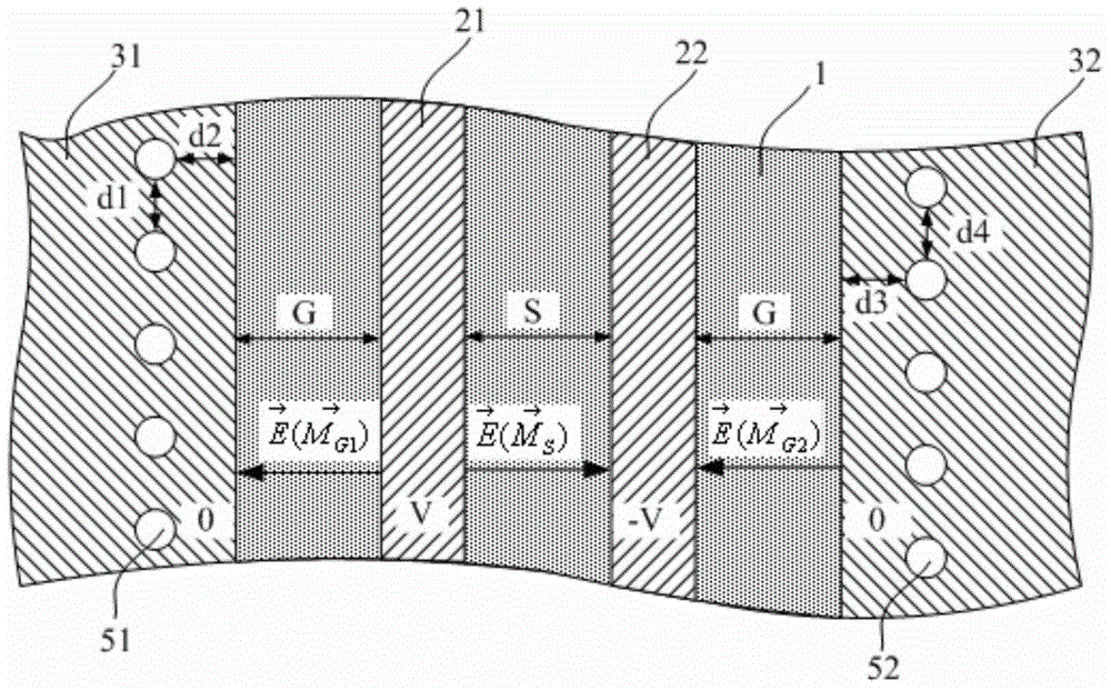
[0024] An embodiment of the present invention provides a circuit board and a method for distributing high-speed differential lines on its surface. The distribution method of the differential lines in the circuit board is an improvement based on the existing coplanar waveguide CPW technology, which can reduce the number of differential lines. Electromagnetic interference generated when transmitting high-frequency signals. The method for distributing the above-m...


PUM


Abstract

The invention relates to the circuit board wiring technology field and discloses a circuit board, a distribution method of surface-layer high-speed difference lines and communication equipment. The circuit board comprises a routing layer, a grounding metal layer and a dielectric layer located between the routing layer and the grounding metal layer. At least one pair of difference lines and ground lines are formed in the routing layer. Two sides of each pair of the difference lines are provided with the ground lines. In the ground lines of the two sides of each pair of the difference lines, the ground lines and the grounding metal layer are connected through a plurality of via holes. In the via hole corresponding to one side ground line, a distance between each via hole and an edge of one side of the one side ground line is less than 2000 micrometers, wherein the edge faces towards one side of the difference line. A distance between the any two adjacent via holes is less than 2000 micrometers. By using the circuit board, an electromagnetic interference generated by the difference lines during high frequency signal transmission can be reduced.

Description

technical field [0001] The invention relates to the technical field of circuit board wiring, in particular to a circuit board and a method for distributing differential lines on its surface. Background technique [0002] In the field of circuit board layout technology, how to reduce the electromagnetic interference of the high-speed transmission line on the surface of the circuit board is an important content of the circuit board layout design. [0003] Taking the packaging substrate as an example, in the packaging substrate, a large part of the electromagnetic interference of the chip is related to the packaging. The electromagnetic interference design of the high-speed IO (Input / Output, input / output) interface is an important content of the packaging substrate design. The current design of high-speed signals, especially differential signals, mainly uses microstrip lines. Microstrip lines are strip-shaped conductors (signal lines) that are isolated from the ground plane by ...

Claims


Application Information

Patent Timeline
Patent Type & Authority Applications(China)
IPC IPC(8): H05K1/02
Inventor 黄慧俞恢春闫美云
Owner HUAWEI TECH CO LTD
Learn More