Cooling chamber and semiconductor processing equipment

A cooling cavity and cooling system technology, applied in semiconductor/solid-state device manufacturing, electrical components, circuits, etc., can solve the problems of increased production cost, long cooling time, low process efficiency, etc., to reduce cooling costs, improve cooling efficiency, The effect of improving process efficiency

Inactive Publication Date: 2015-09-30
BEIJING NAURA MICROELECTRONICS EQUIP CO LTD
View PDF7 Cites 8 Cited by
  • Summary
  • Abstract
  • Description
  • Claims
  • Application Information

AI Technical Summary

Problems solved by technology

[0005] However, the adoption of the above-mentioned cooling chamber will inevitably have the following technical problems in practical applications: in order to reduce the temperature of the substrate S, the cooling gas is continuously delivered to the cooling chamber 10, and the substrate S is continuously absorbed. The cooling gas discharge of heat, that is, the cooling method of heat convection is used to cool the substrate, which makes the heat transfer efficiency low, which not only leads to long cooling time and low process efficiency; Cooling to desired temperature increases production cost

Method used


Image

  • Cooling chamber and semiconductor processing equipment
  • Cooling chamber and semiconductor processing equipment
  • Cooling chamber and semiconductor processing equipment

Examples


Embodiment Construction

[0024] In order for those skilled in the art to better understand the technical solution of the present invention, the cooling chamber and semiconductor processing equipment provided by the present invention will be described in detail below with reference to the accompanying drawings.

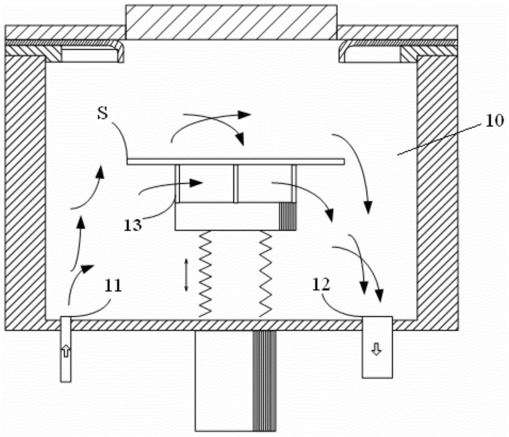
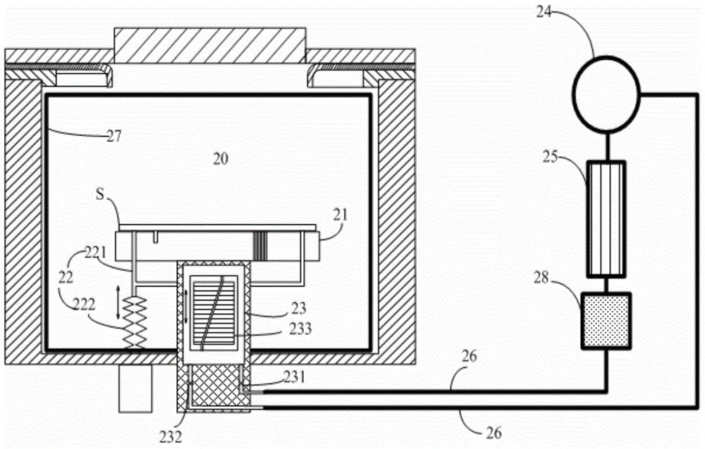
[0025] figure 2 A schematic structural diagram of a cooling chamber provided by an embodiment of the present invention. see figure 2 , the cooling chamber 20 provided by the present invention, the cooling chamber 20 includes a base 21 and a base cooling system, wherein the base 21 is arranged in the cooling chamber 20, and the substrate S to be cooled is placed on the upper surface of the base 21 Above, the pedestal 21 is cooled by means of heat conduction by means of the pedestal cooling system. Specifically, the pedestal cooling system is connected to the lower surface of the pedestal 21, so that the pedestal 21 cools the substrate S to be cooled by heat conduction. Compared with the coo...


PUM


Abstract

The invention provides a cooling chamber and semiconductor processing equipment. The cooling chamber comprises a base and a base cooling system, wherein the base is arranged in the cooling chamber; a to-be-cooled substrate is placed on the upper surface of the base; and the base cooling system is used for cooling the base by adopting a heat conduction mode so as to enable the base to adopt the heat conduction mode for cooling the to-be-cooled substrate. According to the cooling chamber provided by the invention, the cooling efficiency can be improved, the cooling cost can be reduced, and economic benefits can be improved.

Description

technical field [0001] The invention belongs to the technical field of semiconductor equipment manufacturing, in particular to a cooling chamber [0002] and semiconductor processing equipment. Background technique [0003] Physical vapor deposition (Physical Vapor Deposition, hereinafter referred to as PVD) technology is a commonly used processing technology in the field of microelectronics. In the integrated circuit manufacturing industry, it refers to magnetron sputtering technology, which is mainly used for the deposition of metal films such as aluminum and copper. , to obtain metal contacts, metal interconnect lines, etc. [0004] Generally, the PVD process mainly includes three processes: degassing, pre-cleaning and process deposition, and after the process deposition process is completed, due to the high temperature of the substrate, it cannot be directly placed in the cassette and cannot be combined with other non-high temperature resistant However, placing the hig...

Claims


Application Information

Patent Timeline
Patent Type & Authority Applications(China)
IPC IPC(8): H01L21/67
CPCH01L21/67103H01L21/67011
Inventor 刘菲菲
Owner BEIJING NAURA MICROELECTRONICS EQUIP CO LTD
Why Eureka
Try Eureka