Structure and manufacturing method of array colored film integrated type liquid crystal display panel

A technology for liquid crystal display panels and manufacturing methods, applied in nonlinear optics, instruments, optics, etc., can solve the problems of decreased aperture ratio, easy to hide gas, abnormal display, etc., to increase aperture ratio, save photomasks, and reduce production costs Effect

Active Publication Date: 2015-10-07
TCL CHINA STAR OPTOELECTRONICS TECH CO LTD
View PDF4 Cites 36 Cited by
  • Summary
  • Abstract
  • Description
  • Claims
  • Application Information

AI Technical Summary

Problems solved by technology

[0004] However, in the production process of the existing array color filter integrated liquid crystal display panel, holes need to be opened on the color resistance layer for electrically connecting the pixel electrodes to the source / drain electrodes of the TFT. On the one hand, opening holes on the layer will reduce the aperture ratio. On the other hand, opening holes on the color resist layer can easily hide gas. When the liquid crystal display panel encounters high temperature, vibration, or impact, the hidden gas will overflow and form air bubbles. (Bubble), occupying the position of the liquid crystal, causing abnormal display

Method used


Image

  • Structure and manufacturing method of array colored film integrated type liquid crystal display panel
  • Structure and manufacturing method of array colored film integrated type liquid crystal display panel
  • Structure and manufacturing method of array colored film integrated type liquid crystal display panel

Examples


Embodiment Construction

[0035] In order to further illustrate the technical means adopted by the present invention and its effects, the following describes in detail in conjunction with preferred embodiments of the present invention and accompanying drawings.

[0036] see figure 1 , the present invention firstly provides a method for manufacturing an array color filter integrated liquid crystal display panel, comprising the following steps:

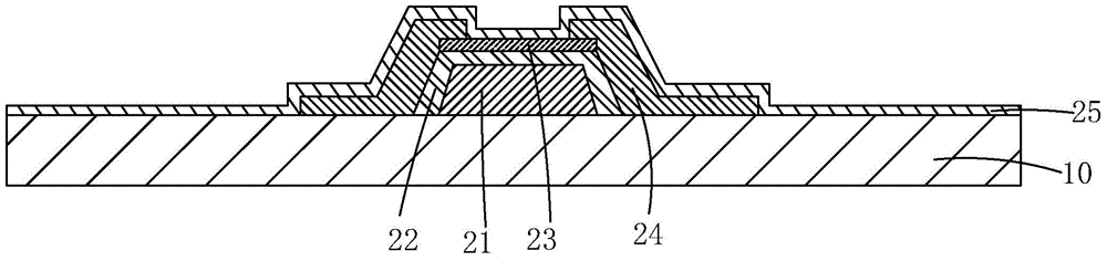
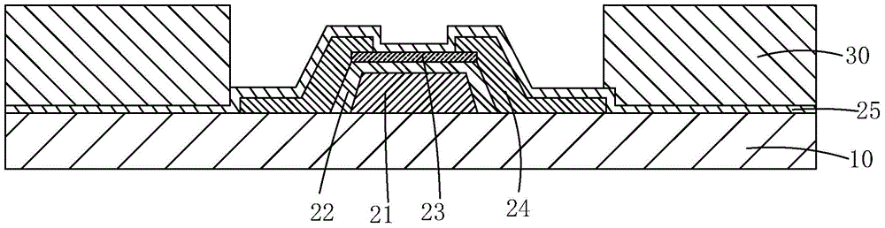
[0037] Step 1. Please refer to figure 2 , providing a first substrate 10, sequentially manufacturing a gate 21, a gate insulating layer 22, a semiconductor layer 23, and a source / drain 24 on the first substrate 10, and then forming a covering source / drain 24, The semiconductor layer 23 and the first protective layer 25 of the first substrate 10 .

[0038]Specifically, the first substrate 10 is preferably a glass substrate; the gate 21 is made by depositing a first metal layer and patterning the first metal layer, and the material of the first metal layer can ...


PUM


Abstract

The invention provides a structure and manufacturing method of an array colored film integrated type liquid crystal display panel. The method includes the steps that a color-shielding layer (30) is manufactured on a first protection layer (25), the portions, located above a grid (21) and a source / drain electrode (24), of the color-shielding layer (30) are removed through a wet etching process, and then a second protection layer (40) covering the color-shielding layer (30) and the first protection layer (25) is deposited; a pixel electrode (50) is formed on the second protection layer (40) and penetrates through a via hole (45) of the second protection layer (40) and the first protection layer (25) to be in contact with the source / drain electrode (24); then the region where the color-shielding layer (30) is removed through the wet etching process is filled with black matrix materials, a black matrix (60) and a spacer (70) located on the black matrix (60) and integrated with the black matrix (60) are manufactured at the same time through a slit mask, the aperture opening ratio can be increased, bubbles are avoided, meanwhile the mask is saved, and the production cost is lowered.

Description

technical field [0001] The invention relates to the technical field of liquid crystal display, in particular to a method for manufacturing an array color filter integrated liquid crystal display panel and its structure. Background technique [0002] With the development of display technology, liquid crystal displays (Liquid Crystal Display, LCD) and other flat display devices are widely used in mobile phones, televisions, personal Various consumer electronic products such as digital assistants, digital cameras, notebook computers, and desktop computers have become the mainstream of display devices. [0003] Most of the liquid crystal displays currently on the market are backlight liquid crystal displays, which include a liquid crystal display panel and a backlight module. Generally, a liquid crystal display panel is composed of a color filter substrate (Color Filter, CF), a thin film transistor array substrate (Thin Film Transistor Array Substrate, TFT Array Substrate), and...

Claims


Application Information

Patent Timeline
Patent Type & Authority Applications(China)
IPC IPC(8): G02F1/1362G02F1/1368G02F1/1335G02F1/1333
CPCG02F1/1333G02F1/136213G02F1/136286G02F1/1368G02F1/13394G02F1/136209G02F1/136227G02F1/13398G02F1/136222G02F1/133516G02F1/1339G02F1/1341G02F1/13439
Inventor 许勇
Owner TCL CHINA STAR OPTOELECTRONICS TECH CO LTD
Why Eureka
Try Eureka