
Pixel control circuit

A technology of pixel control and circuit, used in instruments, static indicators, etc., can solve the problems of image quality degradation, insufficient picture darkness, uneven picture brightness, etc.

Inactive Publication Date: 2015-10-14
AU OPTRONICS CORP
View PDF5 Cites 22 Cited by
  • Summary
  • Abstract
  • Description
  • Claims
  • Application Information

AI Technical Summary

Problems solved by technology

[0004] In this way, although the pixel control circuit 100 can data Controlling the current I flowing through the OLED 110 OLED However, due to the threshold voltage V of the drive transistor T1B TH It may be different due to the difference in the manufacturing process, or it may be changed after a long period of use, so even if each pixel in the display is based on the same data signal S data To display images, the brightness of each pixel may still be uneven due to the different characteristics of the transistor, and the image quality will also decline with time.
[0005] Furthermore, since the pixels in the display are distributed in different positions, the system voltage OVDD received by each pixel may also vary due to the degree of line loss, making the problem of uneven brightness of the screen more difficult to control
[0006] In addition, the pixel control circuit 100 does not provide a discharge path to the OLED 110, so after the previous frame ends, there may be residual charges in the OLED 110, resulting in a black frame when the next frame is black. Not dark enough

Method used


Image

  • Pixel control circuit
  • Pixel control circuit
  • Pixel control circuit

Examples


Embodiment Construction

[0061] The present invention will be described in detail below in conjunction with the accompanying drawings and specific embodiments, but not as a limitation of the present invention.

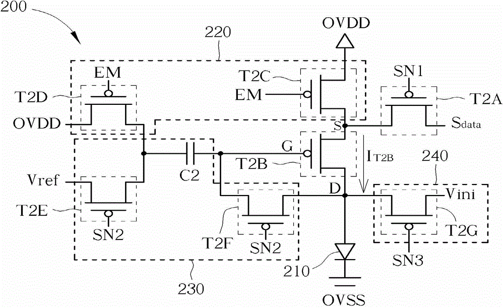
[0062] figure 2 It is a schematic diagram of a pixel control circuit 200 according to an embodiment of the present invention. The pixel control circuit 200 includes an organic light emitting diode 210 , a switch T2A, a driving transistor T2B, a driving circuit 220 , a compensation circuit 230 and a discharge circuit 240 . The organic light emitting diode 210 has a first terminal and a second terminal, and the second terminal of the organic light emitting diode 210 can receive a preset voltage OVSS.

[0063] The switch T2A has a first terminal, a second terminal and a control terminal, and the first terminal of the switch T2A is used for receiving the data signal S data , and the control terminal of the switch T2A is used to receive the first control signal SN1 . The driving transistor T2B ...


PUM


Abstract

The invention discloses a pixel control circuit including an organic LED, a drive transistor, a drive circuit, a discharge circuit and a compensation circuit. The drive transistor is used for conduction or close of the organic LED; the discharge circuit is used for controlling electrical connection between the organic LED and the initial voltage so as to suitably provide an organic LED discharge path; the compensation circuit is used for compensation of the conduction current during the lighting process of the organic LED so as to realize that the conduction current has no relation with the magnitude of the critical voltage of the drive transistor; and the drive circuit is used for controlling electrical connection between the preset voltage and the drive transistor so as to realize lighting of the organic LED.

Description

technical field [0001] The present invention relates to a pixel control circuit, in particular to a pixel control circuit which can prevent pixel luminance from being affected by transistor characteristics. Background technique [0002] figure 1 It is a schematic diagram of a pixel control circuit 100 in the prior art. The pixel control circuit 100 includes a switch T1A, a driving transistor T1B, a capacitor C1 and an organic light emitting diode 110 . The switch T1A has a first terminal, a second terminal and a control terminal, and the first terminal of the switch T1A is used for receiving the data signal S data , and the control terminal of the switch T1A is used to receive the scan signal S scan . The driving transistor T1B has a first terminal, a second terminal and a control terminal, the first terminal of the driving transistor T1B is used to receive the system voltage OVDD, the second terminal of the driving transistor T1B is coupled to the first terminal of the ...

Claims


Application Information

Patent Timeline
Patent Type & Authority Applications(China)
IPC IPC(8): G09G3/32
CPCG09G3/3233G09G2300/0819G09G2300/0842G09G2300/0861
Inventor 洪森全叶佳元
Owner AU OPTRONICS CORP
Learn More