Anti-interference ultrasonic probe

A technology of ultrasonic and piezoelectric wafers, which is applied in the field of ultrasonic probes, can solve the problems of increasing energy loss, affecting measurement accuracy, and affecting resolution, etc., and achieves the effects of reducing pulse width, absorbing clutter, and improving accuracy

Inactive Publication Date: 2015-10-21
CHANGZHOU CHANGCHAO ELECTRONICS RES INSTCO
View PDF15 Cites 3 Cited by
  • Summary
  • Abstract
  • Description
  • Claims
  • Application Information

AI Technical Summary

Problems solved by technology

However, if the vibration time of the piezoelectric chip is too long after the piezoelectric chip starts to vibrate during the working process, the pulse width will be increased and the resolution of the chip will be reduced; Or there will be redundant ultrasonic waves in the front, which will interfere with the normal measurement of the chip, increase energy loss and affect resolution, which will lead to poor resolution during imaging and affect measurement accuracy

Method used


Image

  • Anti-interference ultrasonic probe
  • Anti-interference ultrasonic probe
  • Anti-interference ultrasonic probe

Examples


Embodiment Construction

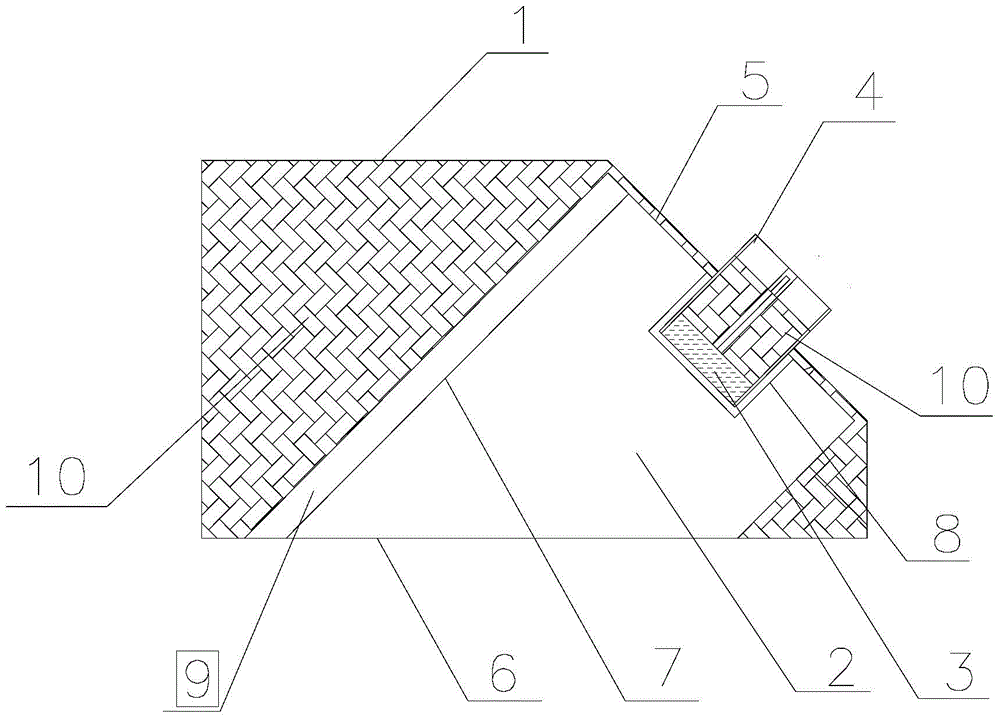
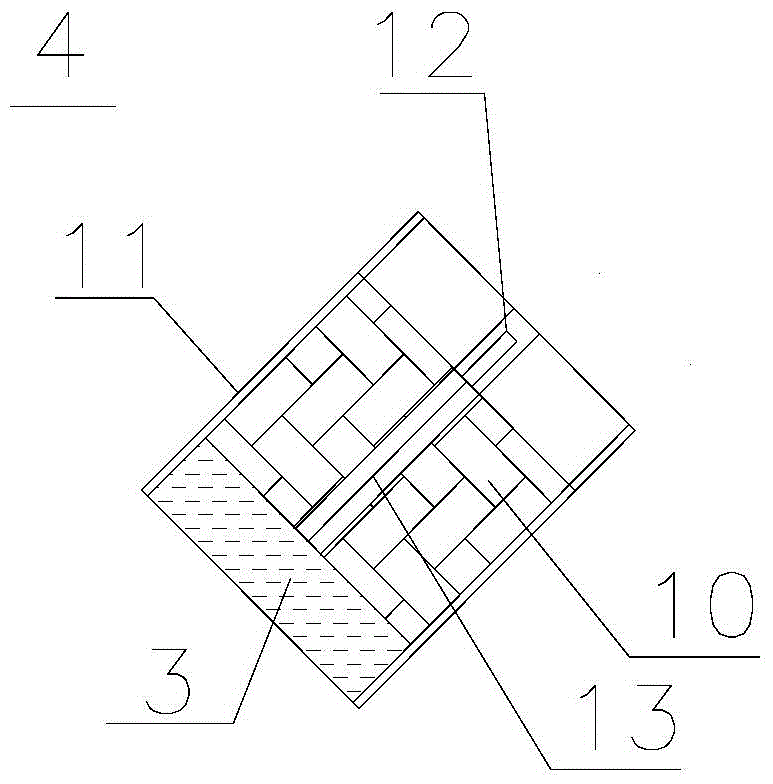
[0018] The present invention will be described in detail in conjunction with accompanying drawing now. This figure is a simplified schematic diagram only illustrating the basic structure of the present invention in a schematic manner, so it only shows the components relevant to the present invention.

[0019] Such as Figure 1-4 As shown, a kind of anti-interference ultrasonic probe of the present invention comprises housing 1, wedge 2, piezoelectric chip 3 and probe interface 4, and wedge 2 is placed in housing 1, and wedge 2 is provided with end face 5, The wedge-shaped surface 6 and the connection surface 7 connected between the end surface 5 and the wedge-shaped surface 6, the end surface 5 is provided with a groove 8, the connection end of the probe interface 4 and the piezoelectric wafer 3 is arranged in the groove 8, the probe interface 4 and the pressure The opposite end of the electric chip 3 extends out of the housing, and the connection surface 7 is provided with a...


PUM


Abstract

The invention provides an anti-interference ultrasonic probe. The anti-interference ultrasonic probe comprises a shell, a wedge block, a piezoelectric wafer and a probe interface, wherein the piezoelectric wafer is connected with the probe interface by a circuit; the wedge block is arranged in the shell and is provided with an end surface, a wedge-shaped surface and a connecting surface connected between the end surface and the wedge-shaped surface; the end surface is provided with a groove; the connecting end of the probe interface and the piezoelectric wafer is arranged in the groove; one end of the probe interface, which is opposite to the piezoelectric wafer, extends out of the shell; the connecting surface is provided with stripy bulges with round and flawed sections; and the planes of the bulges are coincided with the connecting surface. The anti-interference ultrasonic probe provided by the invention has the advantages that the connecting surface of the wedge block is provided with the stripy bulges, and a plurality of surfaces can be utilized for carrying out multi-time reflection and refraction on redundant ultrasonic waves reflected, so that clutter absorption is realized; in addition, the side of the probe interface is provided with absorbing blocks which can suppress the needless vibration of the piezoelectric wafer, so that the pulse width is reduced, the resolution ratio is improved and further the accuracy of measurement is improved.

Description

technical field [0001] The invention relates to the technical field of ultrasonic probes, in particular to an anti-interference ultrasonic probe. Background technique [0002] Ultrasound is a mechanical wave with a vibration frequency higher than that of sound waves, which is generated by the vibration of the transducer chip under the excitation of voltage. It has high frequency, short wavelength, small diffraction phenomenon, especially good directionality, and can be oriented as rays dissemination characteristics. Ultrasound has a great penetrating ability to liquids and solids, especially in solids that are opaque to sunlight, it can penetrate to a depth of tens of meters. Ultrasonic waves will produce significant reflections when they encounter impurities or interfaces to form echoes, and when they encounter moving objects, they will produce Doppler effects. Sensors developed based on ultrasonic characteristics are called "ultrasonic sensors" and are widely used in ind...

Claims


Application Information

Patent Timeline
IPC IPC(8): G01N29/24
Inventor 王钲清
Owner CHANGZHOU CHANGCHAO ELECTRONICS RES INSTCO
Why Eureka
Try Eureka