Semiconductor device with super junction structure, manufacturing method thereof, and photomask

A manufacturing method and semiconductor technology, applied in the field of photolithography, can solve problems such as increased device costs, and achieve the effect of ensuring normal operation

Active Publication Date: 2015-10-21
HANGZHOU SILAN MICROELECTRONICS
View PDF4 Cites 3 Cited by
  • Summary
  • Abstract
  • Description
  • Claims
  • Application Information

AI Technical Summary

Problems solved by technology

In this case, the size of the device will increase, the area will be

Method used


Image

  • Semiconductor device with super junction structure, manufacturing method thereof, and photomask
  • Semiconductor device with super junction structure, manufacturing method thereof, and photomask
  • Semiconductor device with super junction structure, manufacturing method thereof, and photomask

Examples


no. 1 example

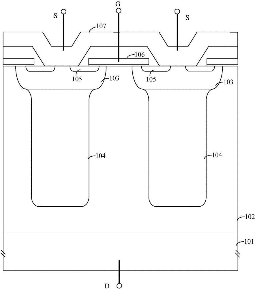
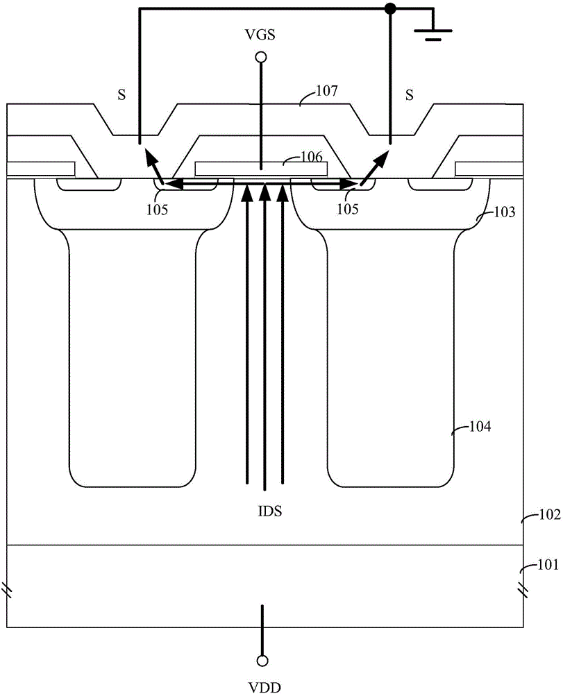
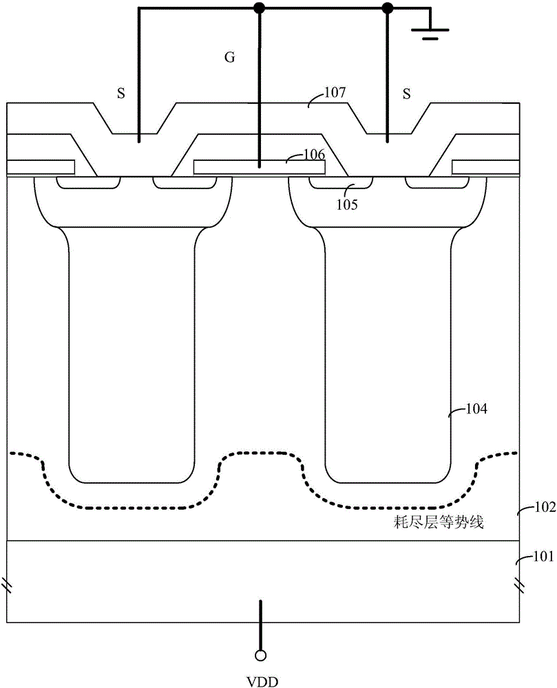
[0087] refer to Figure 6 to Figure 8 , taking a MOS device with a superjunction structure as an example, the layout plane of the device includes an active region 210 and a voltage dividing ring region 211 located on the periphery of the active region, wherein the active region 210 is also called a cell region, and the voltage dividing ring region 211 is also referred to as an area outside the active area.

[0088] The active region 210 has a plurality of first P-type doped regions 220 extending along a first direction (for example, vertically from top to bottom), and a plurality of first P-type doped regions 220 in a second direction (second The directions are arranged at equal intervals in the layout plane perpendicular to the first direction (for example, the transverse direction). There are a plurality of second P-type doped regions 221 extending along the first direction in the pressure dividing ring part 211, and the plurality of second P-type doped regions 221 are arra...

no. 2 example

[0094] refer to Figures 9 to 11 , similar to the first embodiment, still taking a MOS device with a super-junction structure as an example, the layout plane of the device includes an active region 210 and a voltage divider ring region 211 located at the periphery of the active region.

[0095] The active region 210 has a plurality of first P-type doped regions 220 extending along a first direction (for example, vertically from top to bottom), and a plurality of first P-type doped regions 220 in a second direction (second The directions are arranged at equal intervals in the layout plane perpendicular to the first direction (for example, the transverse direction). There are a plurality of second P-type doped regions 221 extending along the first direction in the pressure dividing ring part 211, and the plurality of second P-type doped regions 221 are arranged at equal intervals in the second direction, and the first P-type doped regions The breakdown voltage of the region 220...

no. 3 example

[0101] The manufacturing method of this embodiment can be applied to the super junction structure semiconductor devices shown in the first embodiment and the second embodiment.

[0102] refer to Figure 12 , a semiconductor substrate 201 is provided, and an intermediate sub-epitaxial layer 2021 is formed on the semiconductor substrate 201 . Wherein, the semiconductor substrate 201 can be, for example, an N-type heavily doped (N+) silicon substrate, the intermediate sub-epitaxial layer 2021 is N-type lightly doped (N-), and the intermediate sub-epitaxial layer 2021 can have a preset thickness and Preset resistivity.

[0103] refer to Figure 13 , performing P-type ion implantation on the intermediate sub-epitaxial layer 2021 by using the photolithographic masking layer 2051 , thereby forming P-type doped regions 2031 and 2041 in the intermediate sub-epitaxial layer 2021 . Wherein, the minimum repeat size of the P-type doped region 2031 in the active region is larger, while t...


PUM


Abstract

The invention provides a semiconductor device with a super junction structure, a manufacturing method thereof, and a photomask. The layout plane of the semiconductor device comprises an active region and a potential dividing ring region located at the periphery of the active region. The semiconductor device is characterized in that the active region is internally provided with multiple first P-type doping regions extending along the first direction; the multiple first P-type doping regions are arranged at equal distances in the second direction; the potential dividing ring region is internally provided with multiple second P-type doping regions extending along the first direction; the multiple second P-type doping regions are arranged at equal distances in the second direction; the breakdown voltage of each first P-type doping region is smaller than that of each second P-type doping region; and the second direction is perpendicular to the first direction. Contradiction between conduction resistance and a device area can be overcome, the breakdown point of the device is constantly in the active region, and the device can be ensured to work normally.

Description

technical field [0001] The invention relates to a semiconductor device with a super junction structure, a manufacturing method thereof, and a photolithography plate. Background technique [0002] Compared with planar power MOS devices, high-voltage super-junction MOS devices not only have the characteristics of being able to withstand high withstand voltages, but also have other advantages such as relatively low on-resistance. refer to figure 1 , taking an N-type device as an example, the high-voltage super-junction MOS device mainly includes: a semiconductor substrate 101 , an epitaxial layer 102 , a body region 103 , a P-type doped region 104 , a source region 105 , a gate structure 106 and a metal layer 107 . The difference in structure between the MOS device of the N-type channel superjunction structure and the planar structure MOS device is mainly that there is a P-type doped region 104 under the body region 103 of the former to increase the area of ​​the PN junction, ...

Claims


Application Information

Patent Timeline
IPC IPC(8): H01L29/06H01L21/336H01L21/027
CPCH01L21/027H01L29/0634H01L29/66477
Inventor 李敏张邵华
Owner HANGZHOU SILAN MICROELECTRONICS
Why Eureka
Try Eureka