Method for using gray-tone exposure to generate miniature picture in micro-nano size

A micro-nano and dimensional technology, applied in the field of electron beam lithography, can solve the problems of no obvious advantages in the field of micro-nano structure and the inability to realize irregular pattern preparation, etc., and achieve the effect of high-efficiency nano-pattern manufacturing and high resolution

Inactive Publication Date: 2015-10-28
FUDAN UNIV
View PDF4 Cites 0 Cited by
  • Summary
  • Abstract
  • Description
  • Claims
  • Application Information

AI Technical Summary

Problems solved by technology

Compared with this method, the existing three-dimensional electron beam lithography has the following disadvantages: (1) I

Method used


Image

  • Method for using gray-tone exposure to generate miniature picture in micro-nano size
  • Method for using gray-tone exposure to generate miniature picture in micro-nano size
  • Method for using gray-tone exposure to generate miniature picture in micro-nano size

Examples


Embodiment Construction

[0019] The present invention will be further specifically described below in conjunction with the accompanying drawings and embodiments.

[0020] Concrete operation steps of the present invention are as follows:

[0021] (1) Use Beamer software to form exposure files;

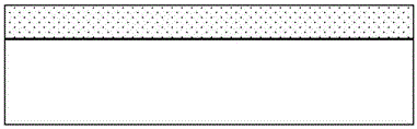
[0022] (2) Clean the silicon substrate, spin-coat PMMA glue with a thickness of 2.5 microns on the substrate, and bake it to harden. The baking temperature is 180 degrees Celsius and the time is 60 minutes. See figure 1 ;

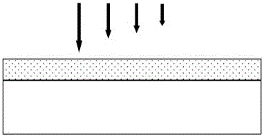
[0023] (3) Use an electron beam lithography machine to expose the designed pattern, see figure 2 ;

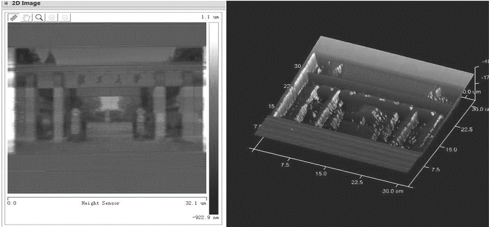
[0024] (4) Develop in 1:1 MIBK and IPA solution at 23 degrees Celsius for 1 minute, then immediately rinse in IPA solution for 30 seconds. Photoresists with different thicknesses have different black and white grayscales after development, thereby generating micro-nano-sized 3D microphotographs, see image 3 , are the AFM top view and oblique view of the finished sample, respectively.


PUM


Abstract

The invention belongs to the technical field of electron-beam lithography, specifically to a method for using gray-tone exposure to generate a miniature picture in the micro-nano size. The method of the invention comprises the steps as follows: firstly using Beamer software to form an exposure file, applying a layer of photoresist to the surface of a silicon wafer through spin-coating, and obtaining the miniature picture in the micro-nano size after development by using the electron-beam lithography. According to the invention, the electron-beam lithography is used to expose the photoresist. The photoresist in different thicknesses has different black and white gray tones after development so as to generate the miniature picture in the micro-nano size. The method of the invention can control the shape of micro-nano graph structure. The generated miniature picture has a nanometer-level resolution ratio, and large area manufacture can be achieved.

Description

technical field [0001] The invention belongs to the technical field of electron beam lithography, and in particular relates to a method for generating micro-nano-sized miniature photos by using the electron beam lithography technology. Background technique [0002] The existing electron beam lithography mainly focuses on the preparation of two-dimensional patterns, although there are several results in the three-dimensional field, mainly in micron-level structures, and because microphotographs have relatively high requirements for precision, roughness, etc., There has been no breakthrough in the micro-nano field. [0003] The preparation of microphotographs of micro-nano size is just one of the applications of this method. Compared with this method, the existing three-dimensional electron beam lithography has the following disadvantages: (1) It cannot realize the preparation of random patterns; (2) It has no obvious advantages in the field of micro-nano structure. Content...

Claims


Application Information

Patent Timeline
IPC IPC(8): B81C1/00
Inventor 陈宜方徐晨
Owner FUDAN UNIV
Why Eureka
Try Eureka