Electrode coating for electron emission devices within cavities

A technology of electron emission and electron emission materials, which is applied in the field of electrode coating of electron emission devices in the cavity, and can solve the problems of time-consuming and expensive

Active Publication Date: 2015-10-28
NEXPERIA BV
View PDF5 Cites 0 Cited by
  • Summary
  • Abstract
  • Description
  • Claims
  • Application Information

AI Technical Summary

Problems solved by technology

Furthermore, said additional process steps are expensive and time-consuming

Method used


Image

  • Electrode coating for electron emission devices within cavities
  • Electrode coating for electron emission devices within cavities
  • Electrode coating for electron emission devices within cavities

Examples


Embodiment Construction

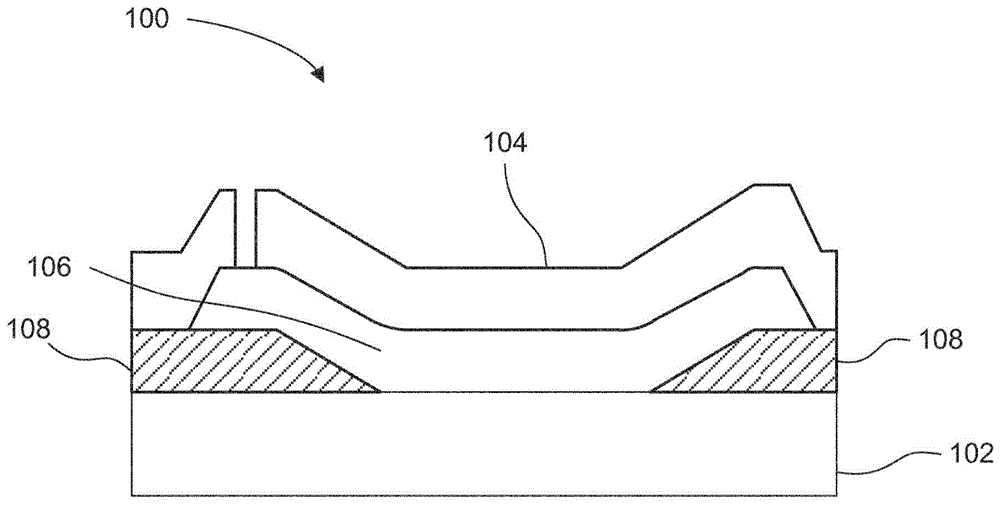
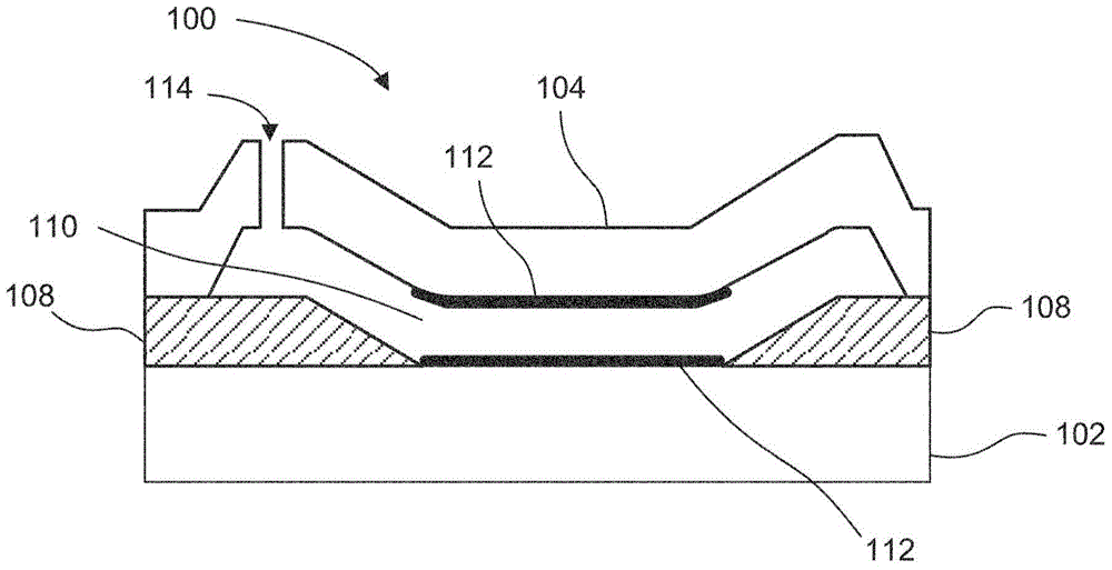
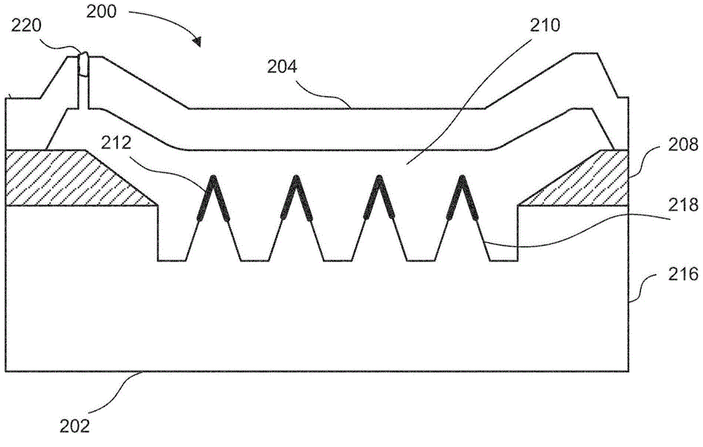
[0024] It should be readily understood that the components of the embodiments mainly described herein and shown in the drawings can be arranged and referred to in many different combinations. Therefore, the following detailed descriptions of various embodiments shown in the drawings are not intended to limit the protection scope of the present invention, but merely represent different embodiments. While various aspects of the embodiments are shown in drawings, the drawings are not necessarily drawn to scale unless explicitly indicated.

[0025]The present invention may embody other specific forms without departing from the spirit or essential characteristics of the invention being invented. The described embodiments are for illustration only and not limitation. The scope of the invention is therefore indicated by the appended claims rather than by the detailed description. All changes in the connotation and range of equivalents fall within the scope of protection claimed by ...


PUM


Abstract

Embodiments of a method for forming a field emission diode for an electrostatic discharge device include forming a first electrode, a sacrificial layer, and a second electrode. The sacrificial layer separates the first and second electrodes. The method further includes forming a cavity between the first and second electrode by removing the sacrificial layer. The cavity separates the first and second electrodes. The method further includes depositing an electron emission material on at least one of the first and second electrodes through at least one access hole after formation of the first and second electrodes. The access hole is located remotely from a location of electron emission on the first and second electrode.

Description

Background technique [0001] Electrostatic discharge is the transfer of electrical current between two charged objects at different electrostatic potentials, and is a reliability and durability problem in solid-state electronics. Electrostatic discharges can be induced by electrostatic fields, or by electrical breakdown, electrical short circuit or simply by contact. Because it can be very destructive, protection against electrostatic discharge is important in many applications. Electrostatic discharge can permanently damage expensive integrated circuits. Therefore, protection from electrostatic discharge is required by an electrostatic discharge protection device. This is especially true for faster and smaller computers that require smaller and newer circuits. Electrostatic discharge can completely destroy faster semiconductor chips. [0002] A common problem with vacuum and quasi-vacuum electronics is the emission of electrons into the cavity, known as field emission or f...

Claims


Application Information

Patent Timeline
Patent Type & Authority Applications(China)
IPC IPC(8): H01J9/12
CPCH01J9/025H01J1/304H01J1/308H01J9/24H01J19/24H01J19/54H01J21/04H01L27/0248
Inventor 克劳斯·莱曼奥拉夫·温尼克迈克尔·安托万·阿曼德·因赞德
Owner NEXPERIA BV
Why Eureka
Try Eureka