Deep Ultraviolet Semiconductor Optical Device

a technology of semiconductors and optical devices, applied in the direction of discharge tubes/lamp details, discharge tubes luminescnet screens, discharge tubes main electrodes, etc., can solve the problem of short-wavelength luminescence of 365 nm, current ultraviolet light sources, and risk of operating loss, etc. problem

Inactive Publication Date: 2010-11-18
YUMEX
View PDF1 Cites 15 Cited by
  • Summary
  • Abstract
  • Description
  • Claims
  • Application Information

AI Technical Summary

Benefits of technology

[0024]According to the present invention, it is possible to obtain a large-area and high-intensity deep ultraviolet light source device in a field emission system.

Problems solved by technology

Therefore, the current ultraviolet light sources have problems such as a risk of operating loss due to short lifetime / vacuum tube rupture or difficulty in downsizing of device chips.
However, as matters stand, high-intensity luminescence cannot be achieved at a short-wavelength of less than 365 nm determined on the basis of a bandgap of gallium nitride.
The reason for this difficulty in achieving high-intensity luminescence is that, although it is necessary to make a structure of a light-emitting diode in which a material of a luminescent active layer is sandwiched by materials with a bandgap higher than that of the luminescent active layer, in order to obtain luminescence out of a deep ultraviolet region, containment of carriers is insufficient even when the luminescent active layer is sandwiched by aluminum nitride with a maximum bandgap, and its luminous efficiency is extremely decreased.
Meanwhile, its luminescent output and external quantum efficiency are low, which results in a situation where the practical use thereof is difficult.
However, EL elements having sufficient performances for practical uses have not yet been realized, that brings about a situation where it is difficult to utilize the EL elements as key devices by applying a luminous phenomenon in an ultraviolet wavelength region to actual products.

Method used


Image

  • Deep Ultraviolet Semiconductor Optical Device
  • Deep Ultraviolet Semiconductor Optical Device
  • Deep Ultraviolet Semiconductor Optical Device

Examples


Embodiment Construction

[0032]Hereinafter, one example of an embodiment of the present invention will be described in detail with reference to the drawings.

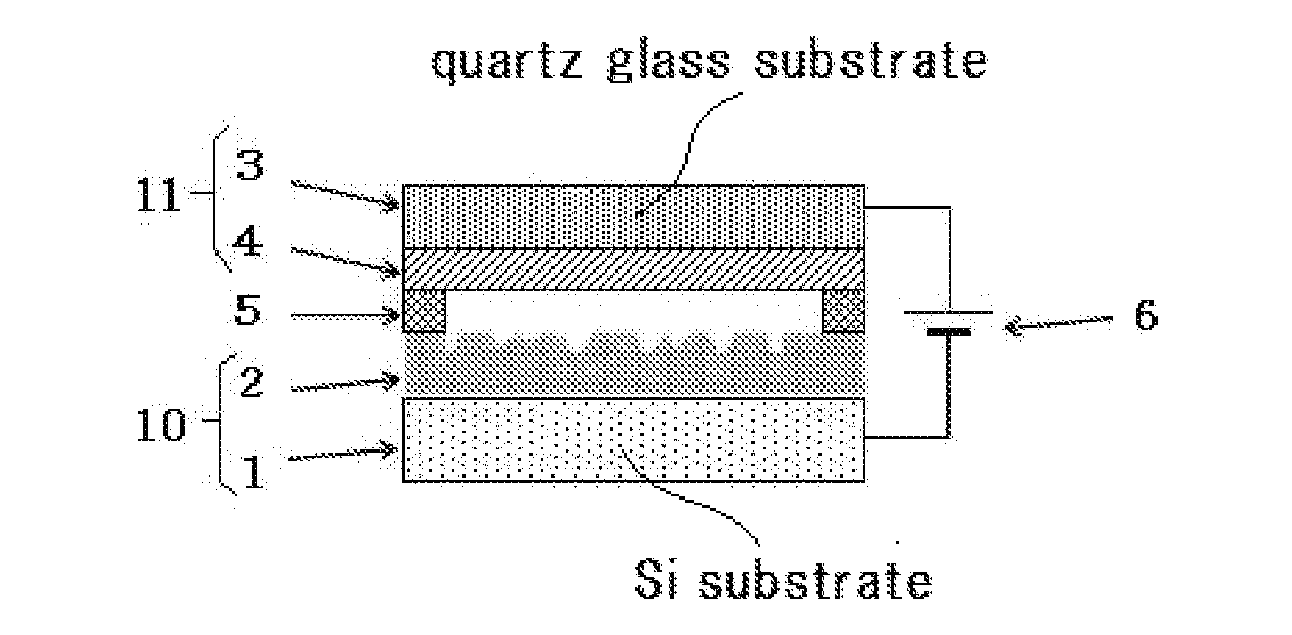
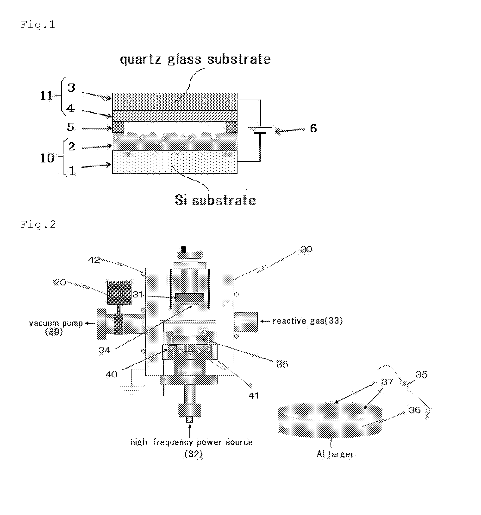
[0033]FIG. 1 shows a structural schematic diagram of a deep ultraviolet light source device according to the present invention. The deep ultraviolet light source device according to the present invention includes at least an Si substrate 1, an Si-doped aluminum nitride (AlN) thin film 2 made to grow at low temperature on the substrate, a quartz glass substrate 3, an ultraviolet phosphor thin film 4 in which gadolinium (Gd) is added to an aluminum nitride serving as a host material, a spacer 5, and a voltage circuit 6.

[0034]Here, the Si-doped AlN thin film 2 made to grow at low temperature on the Si substrate forms an emitter. Further, the Si substrate 1 and the Si-doped AlN thin film 2 form a cathode (negative electrode) 10, the quartz glass substrate 3 and the ultraviolet phosphor thin film 4 form an anode (positive electrode) 11, and the cathode 10 an...


PUM


Abstract

A large-area and high-luminance deep ultraviolet light source device is provided under circumstances where the scales of existing mercury lamps used as ultraviolet light sources cannot be reduced and light-emitting diodes of 365 nm or less do not reach the practical level. The deep ultraviolet light source device comprises at least an anode substrate having an ultraviolet phosphor thin film doped with rare-earth metal ions such as gadolinium (Gd) ions and containing with aluminum nitride as the host material, a cathode substrate having a field electron emission material thin film, a spacer for holding the anode substrate and the cathode substrate opposite to each other and maintaining the space between the substrates in a vacuum atmosphere, and a voltage circuit for applying an electric field to the space between the anode substrate and the cathode substrate. Light is emitted by injecting electrons from the field electron emission material thin film into the ultraviolet phosphor thin film by applying the electric field to the space between the substrates and maintaining the space between the anode substrate and the cathode substrate as a vacuum channel region.

Description

TECHNICAL FIELD[0001]The present invention relates to a deep ultraviolet semiconductor light device, and specifically to a deep ultraviolet field emission device.BACKGROUND ART[0002]Ultraviolet light sources (UV-A, B, C) are not only widely utilized as light sources for exposure, but also expected to be used for environmental / medical fields utilizing the strong antiseptic actions or photochemical reactions, and further to be extensively used for decomposition of environmental pollutants, water quality management, and the like.[0003]At the present time, mercury lamps (with a luminescence ultraviolet wavelength of 254 nm) are mainly used as ultraviolet light sources. In the case of a mercury lamp, its electron source is of a filament type, the light source by electronic excitation naturally becomes a large vacuum-tube device such as a fluorescent lamp. Therefore, the current ultraviolet light sources have problems such as a risk of operating loss due to short lifetime / vacuum tube rupt...

Claims


Application Information

Patent Timeline
Patent Type & Authority Applications(United States)
IPC IPC(8): H01J63/04H05B37/00
CPCC09K11/0883H01J63/04H01J63/06C09K11/7706C09K11/77066
Inventor KITA, TAKASHI
Owner YUMEX
Why Eureka
Try Eureka