Coated carbon nanoflakes

a carbon nanosheet and coating technology, applied in the manufacture of electrode systems, non-metal conductors, electric discharge tubes/lamps, etc., can solve the problems of reducing the local field enhancement factor and the field emission performance of carbon nanosheets, and achieve the effect of improving the effect of electron emission of carbon nanoflakes coated with low z compound

Inactive Publication Date: 2011-07-21
COLLEGE OF WILLIAM & MARY
View PDF5 Cites 16 Cited by
  • Summary
  • Abstract
  • Description
  • Claims
  • Application Information

AI Technical Summary

Benefits of technology

[0008]One embodiment of the invention provides compositions of carbon nanoflakes coated with a low Z compound, where an effective electron emission of the carbon nanoflakes coated with the low Z compound is improved compared to an effective electron emission of the same carbon nanoflakes that are not coated with the low Z compound or of the low Z compound that is not coated onto the carbon nanoflakes.

Problems solved by technology

The conditioning processes, usually time-consuming, lead to degraded field emission performances of carbon nanosheets.
This failure is probably caused by the trade-off between the lower work function of ZrC nanobeads and a decreased local field enhancement factor due to the geometry of these nanobeads.

Method used


Image

  • Coated carbon nanoflakes
  • Coated carbon nanoflakes
  • Coated carbon nanoflakes

Examples


example 1

Synthesis of CrOx—CNS

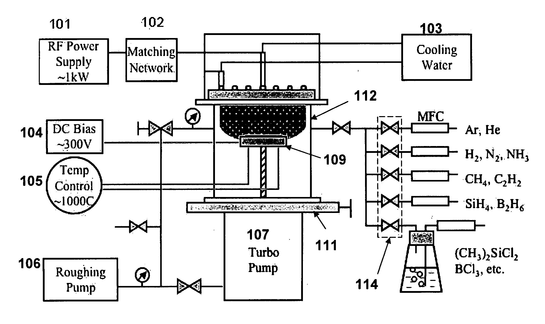
[0054]A four-inch, heavily-doped Si wafer (resistivity of 0.003-0.005 Ω·cm) was loaded on the sample stage (109 as shown in FIG. 1), and the RF-PECVD apparatus was pumped down to 1 mTorr. Hydrogen gas was first introduced into the system at 6 sccm while the substrate was heated up to approximately 700° C., at which temperature it was held for approximately 30 minutes to ensure uniform heating. Then, CH4 was added to the chamber at 4 sccm and the apparatus pressure was stabilized at approximately 100 mTorr. An RF plasma was ignited and tuned as the power was increased to 900 W over the course of about one minute. Deposition was conducted for 20 minutes. The apparatus was cooled down for at least 30 minutes in a hydrogen atmosphere before the sample was taken out.

[0055]The as-grown CNS samples were placed in a vacuum evaporator, and a chromium layer was subsequently evaporated on the surface of the CNS. A tungsten wire twisted into a conical shape was applied as t...

example 2

Characterization of CrOx—CNS

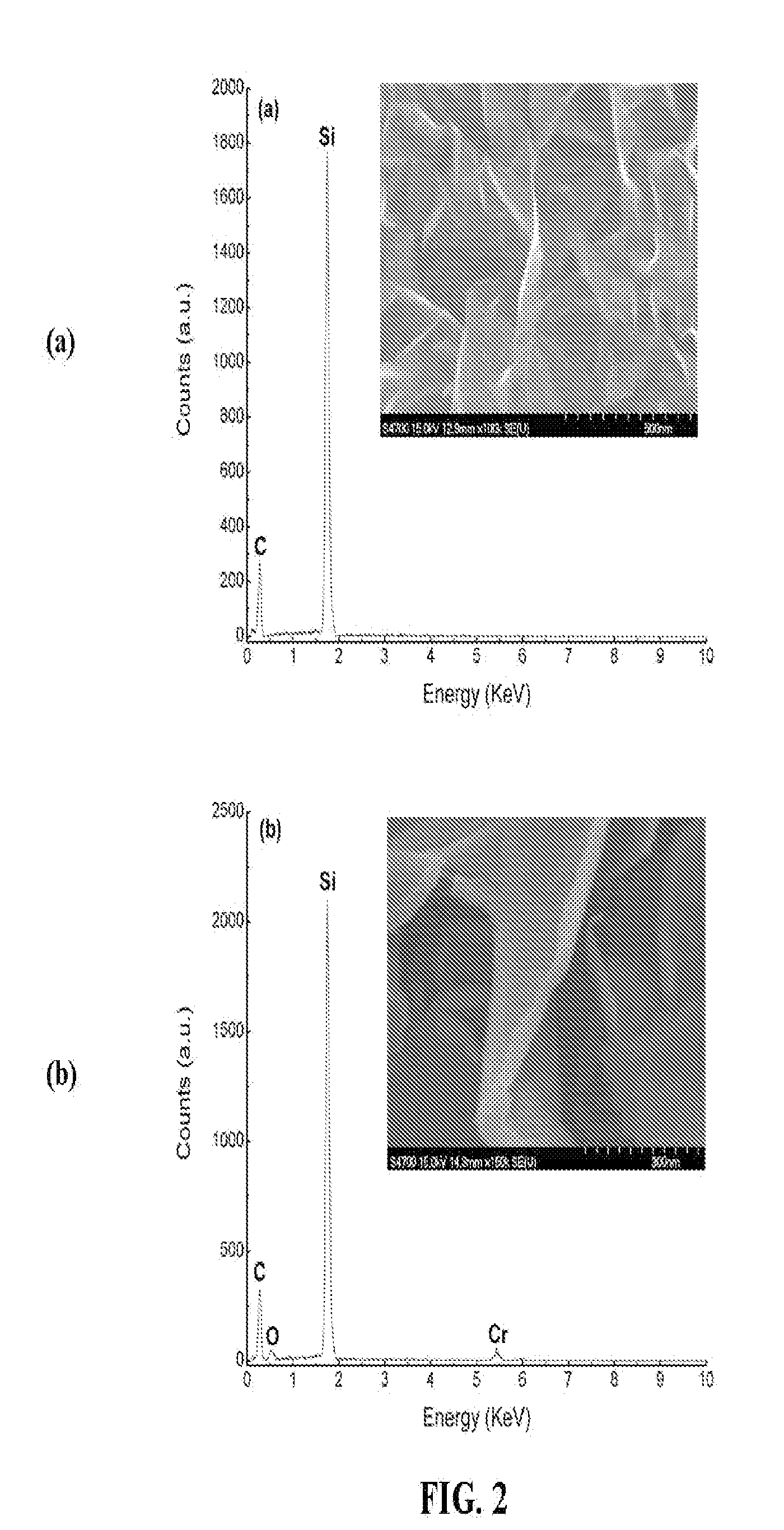
[0056]Elemental analyses of as-grown CNS and CrOx—CNS were conducted by Energy Dispersive X-ray (EDX) analysis accompanied with SEM images. Carbon nanosheets were coated with chromium oxide using 15 seconds evaporation time according to the method of Example 1. FIG. 2a shows the elemental distribution profile extracted from the EDX survey across the sample area of as-grown CNS seen in the SEM image (inset). Peaks associated with C and Si are observed in the profile. The Si peak originates from the substrate on which nanosheets grow and the C peak comes from the CNS. No other elements are detected within this sample area. In contrast to as-grown CNS, the EDX spectrum of CrOx—CNS shown in FIG. 2b not only has peaks associated with C and Si, but also has peaks corresponding to Cr and O, confirming the formation of chromium oxide coating on CNF.

[0057]FIG. 3 shows an Auger spectrum of CrOx—CNS fabricated using 10 seconds chromium evaporation time according to ...

example 3

Field Emission Properties of CrOx—CNS with 15 nm Chromium Oxide Coating

[0060]To directly compare the field emission performance of CrOx—CNS and as-grown CNS, patterned CrOx—CNS samples were used for PEEM and FEEM observations. PEEM captures both photoelectrons generated by the photon source and field emission electrons extracted by the applied electric field to form images while FEEM only uses field emission electrons for imaging with the absence of photon source in PEEM. The contrast information of PEEM and FEEM images yields the spatial distributions of electron source in the sample and thereby determines the emission uniformity of the sample. Patterned CrOx—CNS samples were fabricated by using an evaporation time of 10 seconds through a TEM grid that was placed over as-grown CNS samples, resulting in a sample consisting of alternating CrOx—CNS squares and as-grown CNS streets. PEEM systems operating at pressures on the order of ˜10−8 Torr were used to conduct these observations w...


PUM

PropertyMeasurementUnit
thicknessaaaaaaaaaa
thicknessaaaaaaaaaa
thicknessaaaaaaaaaa

Abstract

Compositions of carbon nanoflakes are coated with a low Z compound, where an effective electron emission of the carbon nanoflakes coated with the low Z compound is improved compared to an effective electron emission of the same carbon nanoflakes that are not coated with the low Z compound or of the low Z compound that is not coated onto the carbon nanoflakes. Compositions of chromium oxide and molybdenum carbide-coated carbon nanoflakes are also described, as well as applications of these compositions. Carbon nanoflakes are formed and a low Z compound coating, such as a chromium oxide or molybdenum carbide coating, is formed on the surfaces of carbon nanoflakes. The coated carbon nanoflakes have excellent field emission properties.

Description

CROSS-REFERENCE TO RELATED APPLICATIONS[0001]This Application claims priority to U.S. Provisional application Ser. No. 61 / 024,071, filed on Jan. 28, 2008, and US Provisional application titled “Coated Carbon Nanoflakes” (attorney docket no. 047911 / 0108), filed on Jan. 14, 2009, both of which are incorporated herein by reference in their entirety.STATEMENT REGARDING FEDERALLY SPONSORED RESEARCH AND DEVELOPMENT[0002]This invention was made with Government support under Grant No. N00014-05-1-0749 awarded by the Office of Naval Research. The Government has certain rights in the invention.FIELD OF INVENTION[0003]The field of the invention relates to compositions of coated carbon nanoflakes and applications thereof, particularly for vacuum microelectronics.BACKGROUND OF THE INVENTION[0004]High current with sufficient current density, long lifetime, good emission stability and spatial uniformity are general requirements of cold cathode materials for application in vacuum microelectronic de...

Claims


Application Information

Patent Timeline
Patent Type & Authority Applications(United States)
IPC IPC(8): H01B1/04H01B1/02B05D5/12B05D3/10B82Y30/00B82Y40/00
CPCB82Y30/00B82Y40/00C01B31/04C23C14/18C23C14/5806C23C14/5853H01J2201/30496H01J9/025H01J2201/30453H01J2201/30484H01J2201/30488H01J2201/30492H01J1/304
Inventor HOU, KUNMANOS, DENNIS M.OUTLAW, RONALD A.
Owner COLLEGE OF WILLIAM & MARY
Why Eureka
Try Eureka