Electron emitting device

a technology of electron emitting device and electron, which is applied in the direction of electric discharge tube/lamp manufacture, discharge tube luminescnet screen, therapy, etc., can solve the problems of electrons losing their energy, poor crystallinity of diamond, and not effectively injecting electrons into diamond particles on the surface, so as to reduce the energy band of space charge region, reduce the effect of crystal defects or the like in the interface, and low barrier sta

Inactive Publication Date: 2005-06-23
SUMITOMO ELECTRIC IND LTD
View PDF10 Cites 15 Cited by
  • Summary
  • Abstract
  • Description
  • Claims
  • Application Information

AI Technical Summary

Benefits of technology

[0010] The electron emission portion constituting a part of the projection may have a tip layer comprised of a p-type diamond, and an intermediate layer comprised of a non-doped diamond provided between the tip layer and the base. In this configuration, the space charge region, which is formed in the area including the interface (a junction interface between the n-type diamond and the non-doped diamond) between the base and the electron emission portion (the intermediate layer), is located on the tip side rather than in the root region of the projection. In this case, when electrons are emitted from the electron emitting device by an electric field, the electric field also becomes more likely to be exerted on the projection, without need for provision of the electrode as required in the electron emitting device described in above Document 3. In other words, the electric field readily penetrates the interior of the projection to lower the energy band of the space charge region, so as to establish a low barrier state. This matter means that electrons in the n-type diamond forming the base come to be effectively injected into the conduction band of the diamond forming the electron emission portion. After electrons are injected into the conduction band of the diamond, the electrons rarely lose their energy inside the projection because of scattering or the like, and adequately come to reach the surface of the electron emission portion. Furthermore, since the intermediate layer of the non-doped diamond is provided, it is feasible to decrease crystal defects or the like in the interface and thus to prevent loss of energy during passage of electrons through the interface. As a result, the electron emitting device efficiently emits electrons from the tip of the electron emission portion.
[0011] In the electron emitting device according to the present invention, a height of the electron emission portion, which is defined by a distance from the tip of the projection to the interface between the base and the electron emission portion, is preferably 100 nm or less. In this case, the space charge region formed in the area including the junction interface between the different kinds of diamonds is located in the vicinity of the tip of the projection. For this reason, when electrons are emitted from the electron emitting device by an electric field, the electric field adequately penetrates the interior of the projection to effectively lower the energy band of the space charge region. As a result, electrons are efficiently emitted from the tip of the electron emission portion. This distance permits the electrons injected into the base of the projection to reach the tip of the electron emitting device without loss of energy due to scattering or the like, whereby the electrons can be emitted more effectively.
[0012] In the electron emitting device according to the present invention, the height of the electron emission portion, defined by the distance from the tip of the projection to the interface between the base and the electron emission portion, is preferably not more than a width of the space charge region formed in the area including the interface between the base and the electron emission portion. In this case, since the distance from the tip of the projection to the interface between the base and the electron emission portion becomes sufficiently short, the space charge region is located in the vicinity of the tip of the projection. Therefore, when electrons are emitted from the electron emitting device by an electric field, the electric field adequately penetrates the interior of the projection to effectively lower the energy band of the space charge region. As a result, the electron emitting device further efficiently emits electrons from the tip of the electron emission portion.
[0013] In the electron emitting device according to the present invention, the interface between the base and the electron emission portion or the interface between the base and the intermediate layer is preferably exposed in a vacuum space. This configuration permits the electric field to effectively intrude into the interface as well, whereby the energy band of the space charge region is lowered, so as to increase the electron emission efficiency.
[0014] Furthermore, the electron emitting device according to the present invention preferably further comprises an electroconductive material covering at least a side face of the base. In this configuration, when a voltage is applied between the electron emitting device and an electrode such as an anode, electrons are sufficiently supplied into the n-type diamond forming the base. Since the electroconductive material part wholly becomes equipotential, it is feasible to increase the intensity of the electric field penetrating the interior of the projection in an end region of the electroconductive material at the tip of the projection.
[0015] In the electron emitting device according to the present invention, a distance (a distance along a height direction of the electron emission portion), from an end of the electroconductive material to the interface between the base and the electron emission portion or to the interface between the base and the intermediate layer, is set in a certain range. Here, when R represents a maximum size of the projection at the interface (in the case where the projection is conical, the maximum size is a diameter of the interface) and L a minimum distance along the height direction of the electron emission portion from the interface to the end of the electroconductive material, the electron emitting device preferably satisfies a condition of L<R or a condition of L<1000 nm. When the condition of L<R is satisfied, a precipitous electric field is exerted on the depletion region at the interface. When the condition of L<1000 nm is satisfied, the distance L becomes shorter than the free path of electrons under a high electric field, and it is thus feasible to suppress carrier loss due to recombination and to efficiently inject electrons into the electron emission portion.

Problems solved by technology

Namely, the electron emitting device described in above Document 1 has the problem that electrons are not effectively injected into diamond particles in the surface, and electrons existing not in the conduction band of diamond but in the valence band in fact are considered to be emitted by a strong electric field.
The electron emitting device described in above Document 2 has the problem that the crystallinity of diamond is poor and even when electrons are injected into the conduction band of diamond, the electrons will lose their energy because of scattering, recombination, and so on.
For this reason, electrons can fail to reach the surface of the cathode in the electron emitting device described in above Document 2, and are considered not to effectively contribute to electron emission.
Therefore, the electron emitting device described in above Document 3 has the problem of complicated structure and the problem of power consumption caused by a bias for driving.

Method used


Image

  • Electron emitting device
  • Electron emitting device
  • Electron emitting device

Examples


first embodiment

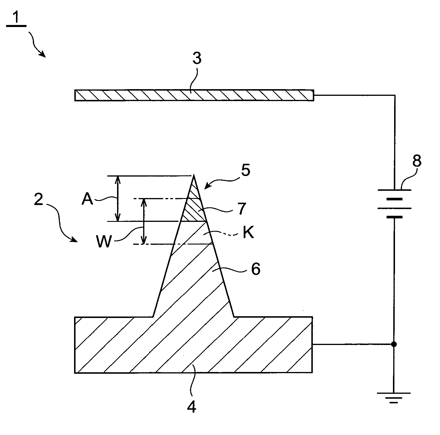
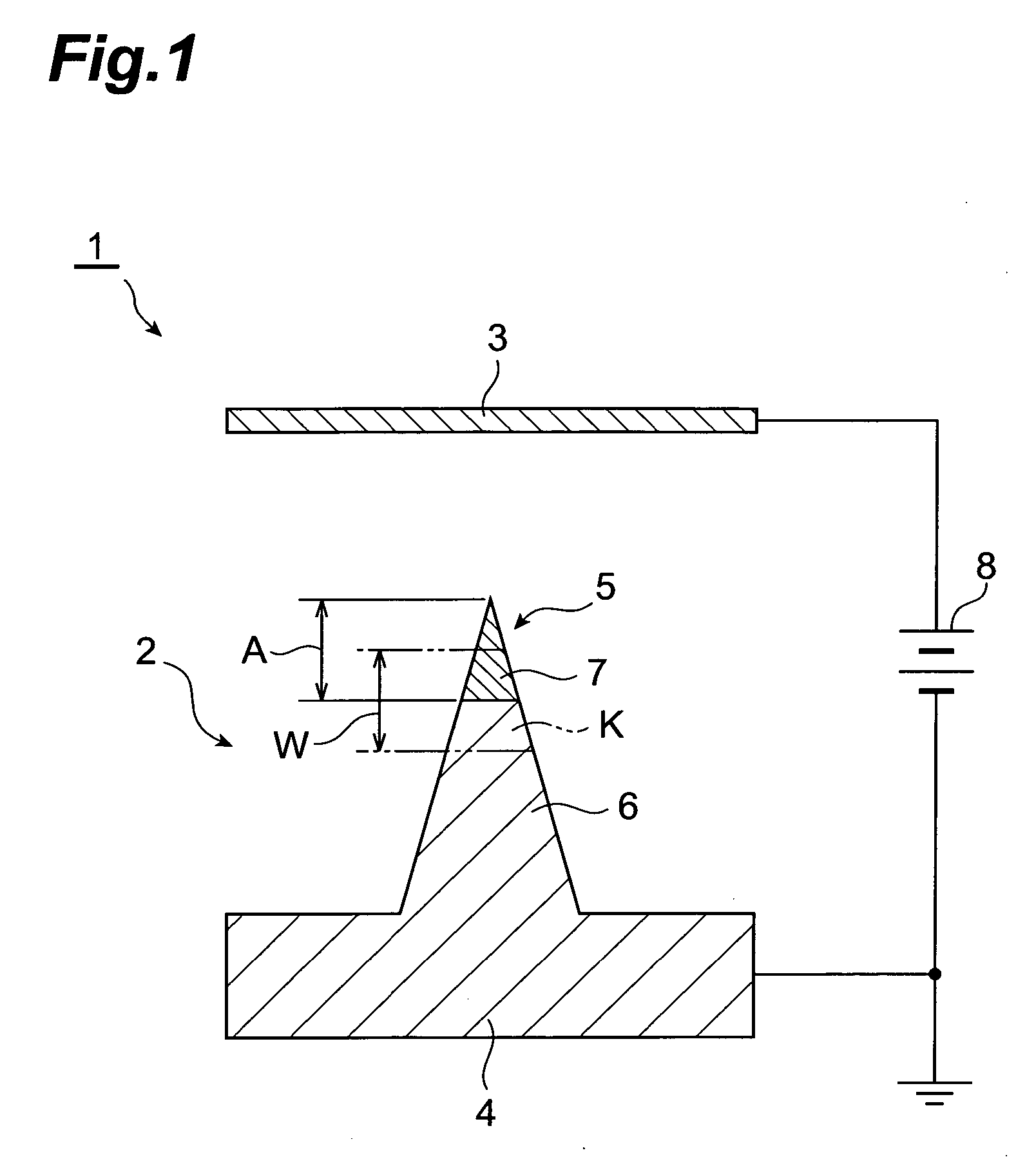
[0035]FIG. 1 is a sectional view showing a configuration of an electron beam source having the electron emitting device according to the present invention. In this FIG. 1, the electron beam source 1 has an electron emitting device 2 made of diamonds, and a positive electrode (anode) 3 placed opposite to this electron emitting device 2. The electron emitting device 2 and anode 3 are installed in a vacuum chamber.

[0036] The electron emitting device 2 has a substrate 4 made of an n-type diamond, and a plurality of projections 5 (only one of which is shown in FIG. 1) formed on the substrate 4. The projections 5 have a pointed shape such as a conical shape or a quadrangular pyramid.

[0037] The projection 5 comprises a base 6 provided on the substrate 4 side, and an electron emission portion 7 provided on the base 6 and emitting electrons from its tip. The base 6 is made of an n-type diamond in similar to the substrate 4. The electron emission portion 7 is made of a p-type diamond.

[0038]...

third embodiment

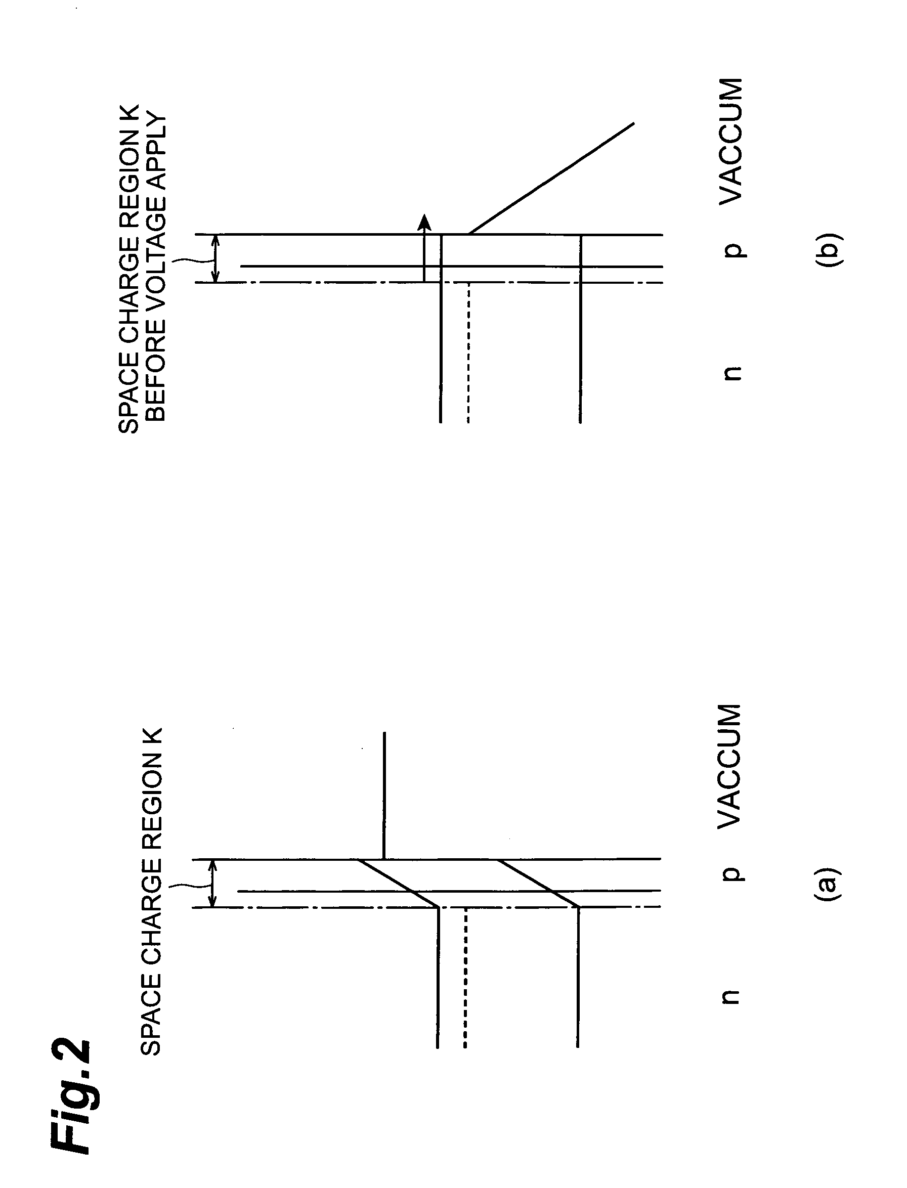
[0062] Here, the distance L between the edge of the electroconductive material and the interface (the distance along the height direction of the electron emission portion 7) preferably satisfies the condition of L5 at the interface. In this third embodiment, the diameter of the interface is 300 nm and the distance L 200 nm.

[0063]FIG. 10 is a sectional view showing a configuration of an electron beam source having the fourth embodiment of the electron emitting device according to the present invention. In this FIG. 10 the electron beam source 30 has the electron emitting device 31 according to the fourth embodiment. The electron emitting device 31 according to the fourth embodiment also has the substrate 4 and projection 5 of the same structure as those in the electron emitting device 1 according to the first embodiment. The electron emitting device 31 according to the fourth embodiment is, however, different from the first embodiment in that it is provided with a gate electrode 33 t...


PUM


Abstract

The present invention relates to an electron emitting device having a structure for efficiently emitting electrons. The electron emitting device has a substrate comprised of an n-type diamond, and a pointed projection provided on the substrate. The projection comprises a base provided on the substrate side, and an electron emission portion provided on the base and emitting electrons from the tip thereof. The base is comprised of an n-type diamond. The electron emission portion is comprised of a p-type diamond. The length from the tip of the projection (electron emission portion) to the interface between the base and the electron emission portion is preferably 100 nm or less.

Description

BACKGROUND OF THE INVENTION [0001] 1. Field of the Invention [0002] The present invention relates to an electron emitting device extensively applicable to such apparatus as high-frequency amplifiers, microwave oscillators, light emitting devices, and electron beam lithography apparatus. [0003] 2. Related Background Art [0004] The conventional electron emitting devices (electron sources) having been used heretofore include thermionic emission sources using a tungsten filament, cold cathodes using lanthanum hexaboride, thermal-field emission cathodes using zirconia-coated tungsten, and so on. Among materials applied to these electron emitting devices, diamond is drawing attention in recent years because of possession of negative electron affinity. Examples of the known electron emitting devices of this type include the electron emitting device in which a metal cathode is coated with diamond, as described in Journal of Vacuum Science and Technology B 14 (1996) 2060 (Document 1), the el...

Claims


Application Information

Patent Timeline
Patent Type & Authority Applications(United States)
IPC IPC(8): H01J1/304H01J1/308H01J63/02
CPCH01J1/3044H01J63/02H01J1/308
Inventor TATSUMI, NATSUONAMBA, AKIHIKONISHIBAYASHI, YOSHIKIIMAI, TAKAHIRO
Owner SUMITOMO ELECTRIC IND LTD
Why Eureka
Try Eureka