Method for producing electron-emitting device and method for producing image display apparatus including the same
a technology of electron emission and image display, which is applied in the manufacture of electric discharge tubes/lamps, cold cathode manufacturing, and electromechanical systems, etc., can solve problems such as unplanned current flow, and achieve the effects of enhancing the efficiency of electron emission, and reducing the risk of leakage curren
- Summary
- Abstract
- Description
- Claims
- Application Information
AI Technical Summary
Benefits of technology
Problems solved by technology
Method used
Image
Examples
example 1
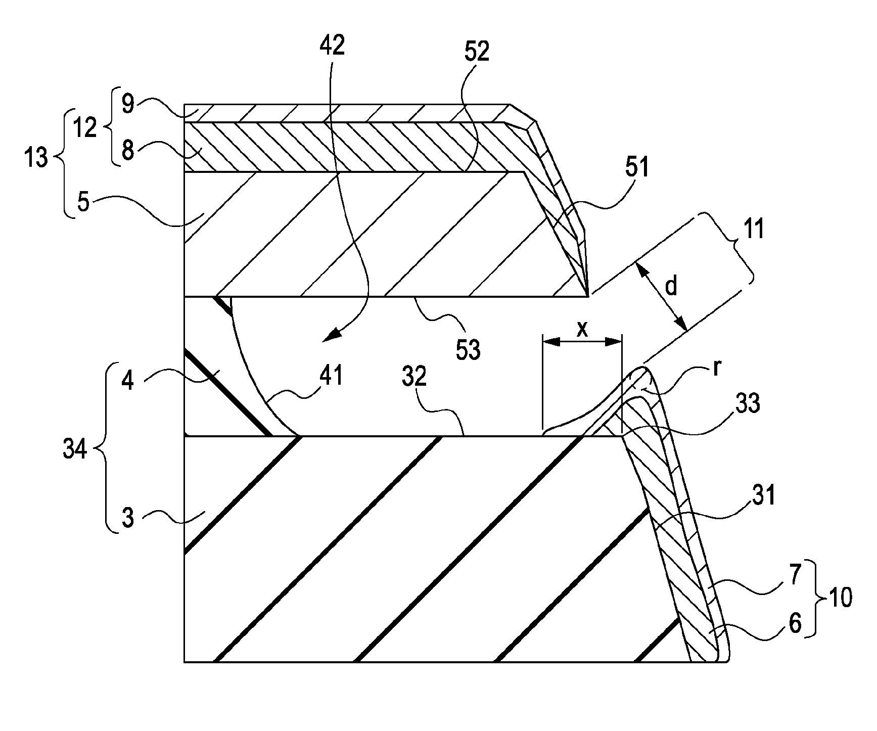
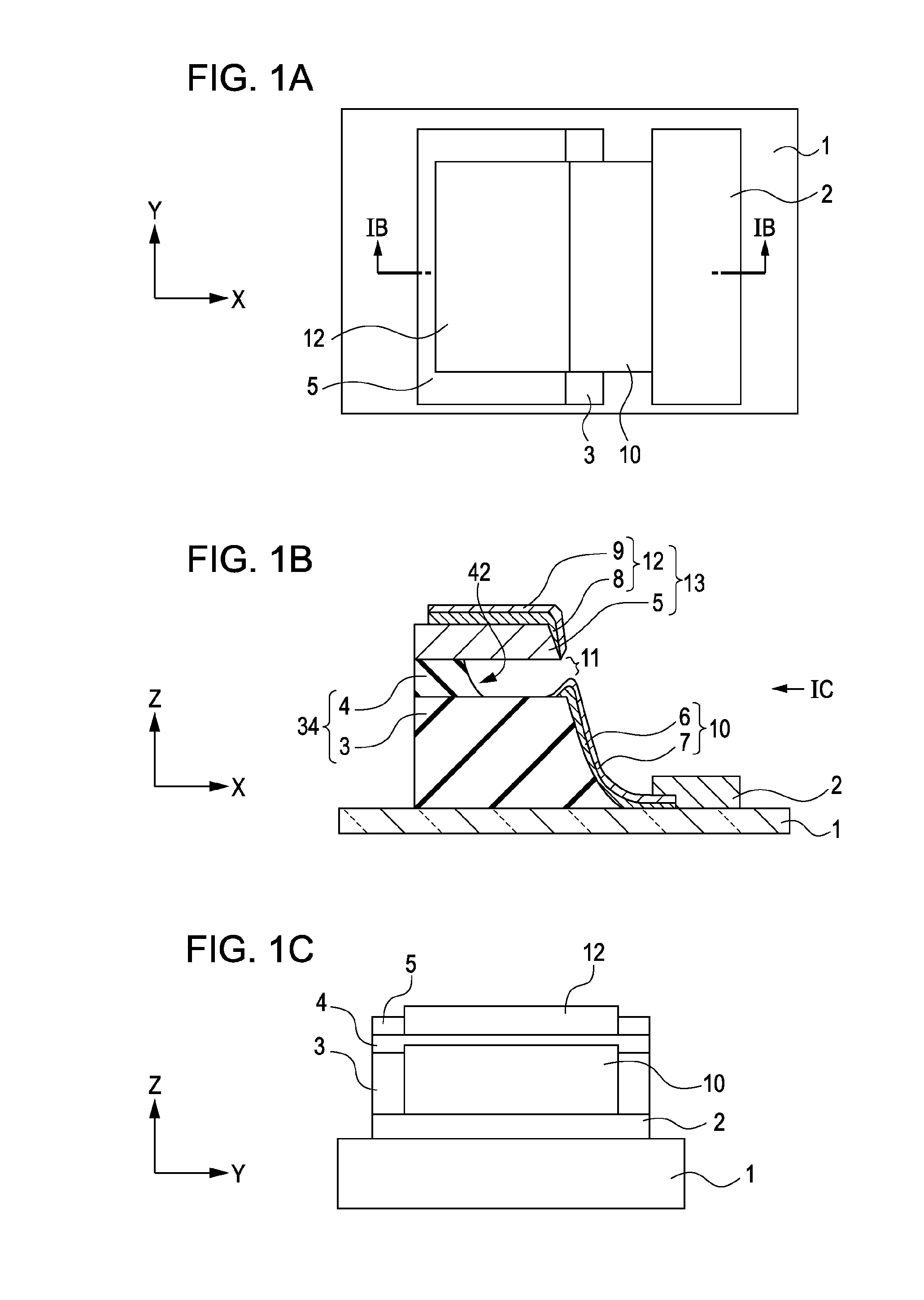
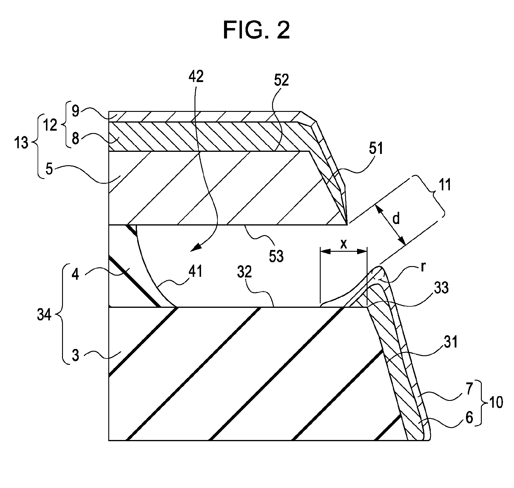
[0158]An example of a method for producing an electron-emitting device according to an embodiment of the present invention will be described with reference to FIGS. 4A to 5C. FIGS. 4A to 5C are schematic views sequentially illustrating steps for producing an electron-emitting device according to an embodiment of the present invention.
[0159]Referring to FIG. 4A, the insulation layers 30 and 40 and the conductive layer 50 were stacked on the substrate 1. The substrate 1 was composed of high-strain-point low-sodium glass (PD200 manufactured by Asahi Glass Co., Ltd.).
[0160]As for the insulation layer 30, a Si3N4 film that was composed of a material having excellent processability and served as an insulation film was formed by a sputtering method. The insulation layer 30 had a thickness of 500 nm. As for the insulation layer 40, a SiO2 film that was composed of a material having excellent processability and served as an insulation film was formed by a sputtering method. The insulation la...
example 2
[0178]Example 2 was the same as Example 1 except that the second-step film formation in Example 1 was changed, and hence, the production method of Example 2 will be described only in terms of the second-step film formation, which was different from Example 1.
[0179]As the second-step film formation, non-collimated sputtering in which the distribution of angles at which a film-formation material (Mo particles) is applied is large was conducted. As a result, the second conductive film 7 having a film density higher than the film density of a portion of the first conductive film 6 on the inclined surface 31 of the first insulation layer 3 (the portion being formed in the first-step film formation) was formed so as to cover the portion of the first conductive film 6 on the inclined surface 31.
[0180]Note that, when the first conductive film 6 is formed only by non-collimated sputtering, the first conductive film 6 having good quality can be formed on the inclined surface 31. However, in t...
example 3
[0183]Example 3 was the same as Example 1 except that the two-step film formation in Example 1 was changed, and hence, the production method of Example 3 will be described only in terms of the two-step film formation, which was different from Example 1.
[0184]As a first-step film formation, Mo was applied in a direction perpendicular to the surface of the substrate 1 (a direction of a line normal to the top surface 32) by collimated sputtering in which the distribution of angles at which the film-formation material (Mo particles) was applied to the surface on which a film was to be formed was made small. As a result, the first conductive film 6 and the third conductive film 8 were formed. At this time, a projected portion was formed at an end portion of the first conductive film 6. The first conductive film 6 and the third conductive film 8 were not connected to each other. The first conductive film 6 and the gate electrode 5 were not connected to each other.
[0185]As the second-step ...
PUM
 Abstract
Description
Claims
Application Information


