
Electron emission device and electron emission display using the electron emission device

Inactive Publication Date: 2006-11-30
SAMSUNG SDI CO LTD
View PDF10 Cites 5 Cited by
  • Summary
  • Abstract
  • Description
  • Claims
  • Application Information

AI Technical Summary

Benefits of technology

[0010] It is therefore a feature of an embodiment of the present invention to provide an electron emission device configured to exhibit efficient emission of electrons from electron emission regions by effectively forming an electric field around the electron emission regions.
[0011] It is therefore another feature of an embodiment of the present invention to provide an electron emission display configured to operate with a relatively low driving voltage, which may increase the service life of the electron emission regions and the display.

Problems solved by technology

A drawback to the above-described FEA electron emission device is that it may be difficult to properly form the electric field around the electron emission regions.
As a result, electrons may be primarily emitted from the local region of the electron emission region, which may lower the efficiency of electron emission.
However, the increased driving voltage may reduce the service life of the electron emission regions.
Therefore, the above-described FEA electron emission device may not be suitable for a high-efficiency electron emission display.

Method used


Image

  • Electron emission device and electron emission display using the electron emission device
  • Electron emission device and electron emission display using the electron emission device
  • Electron emission device and electron emission display using the electron emission device

Examples


first embodiment

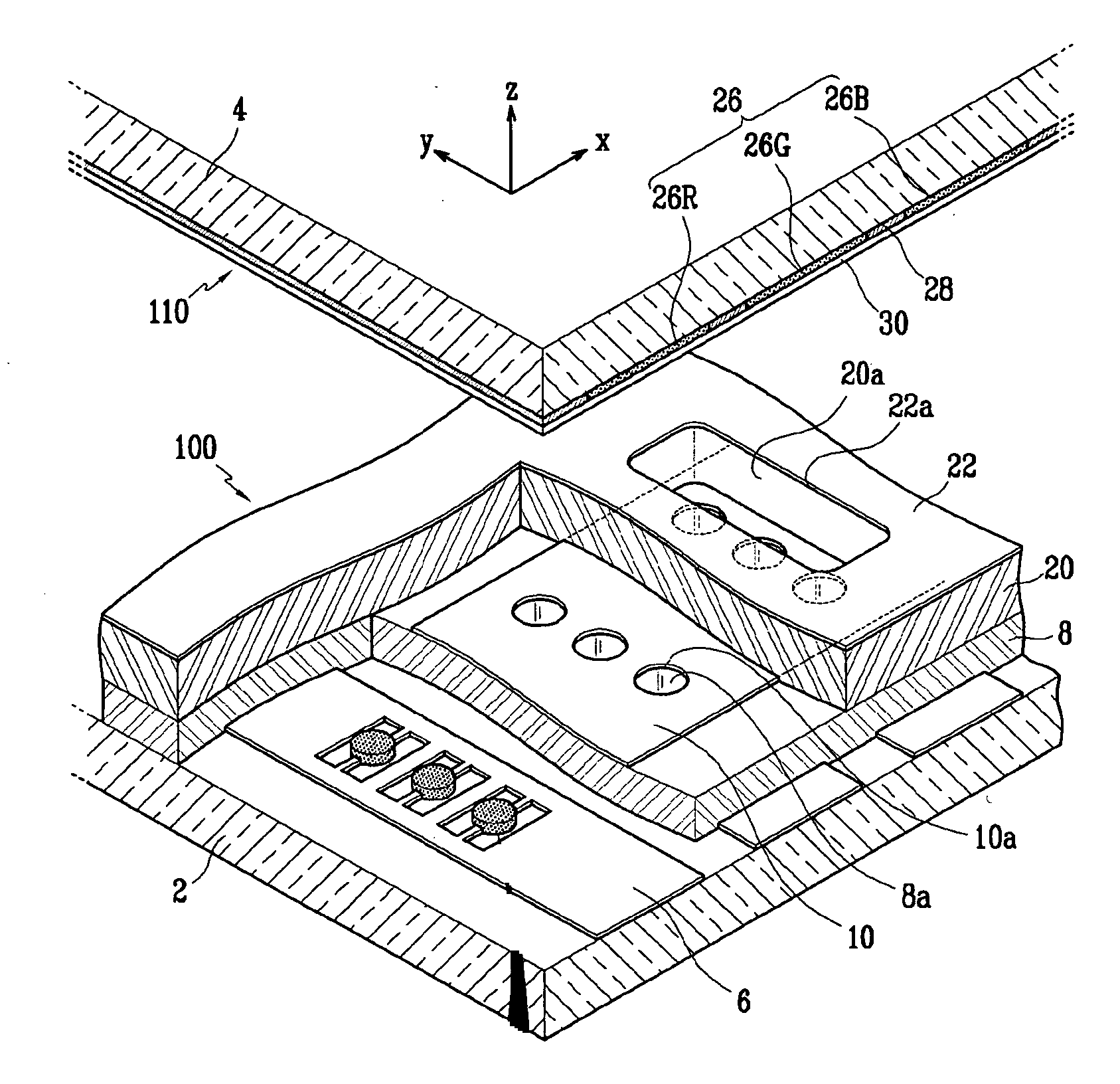
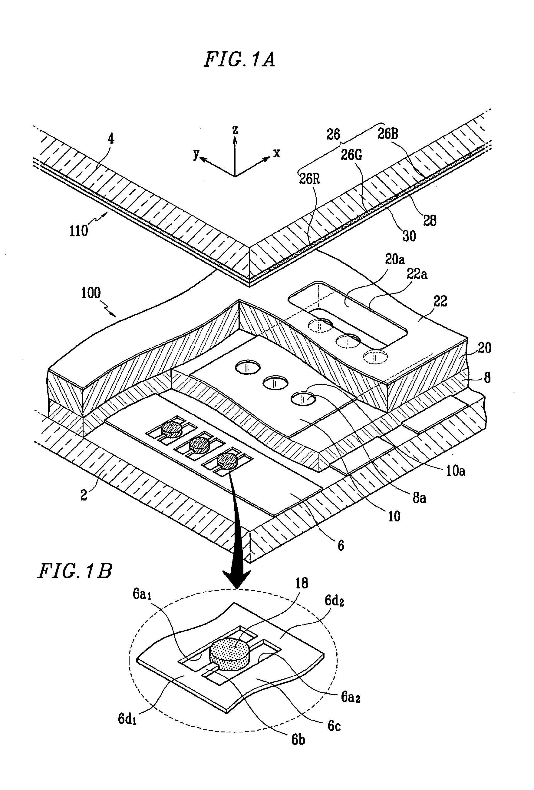
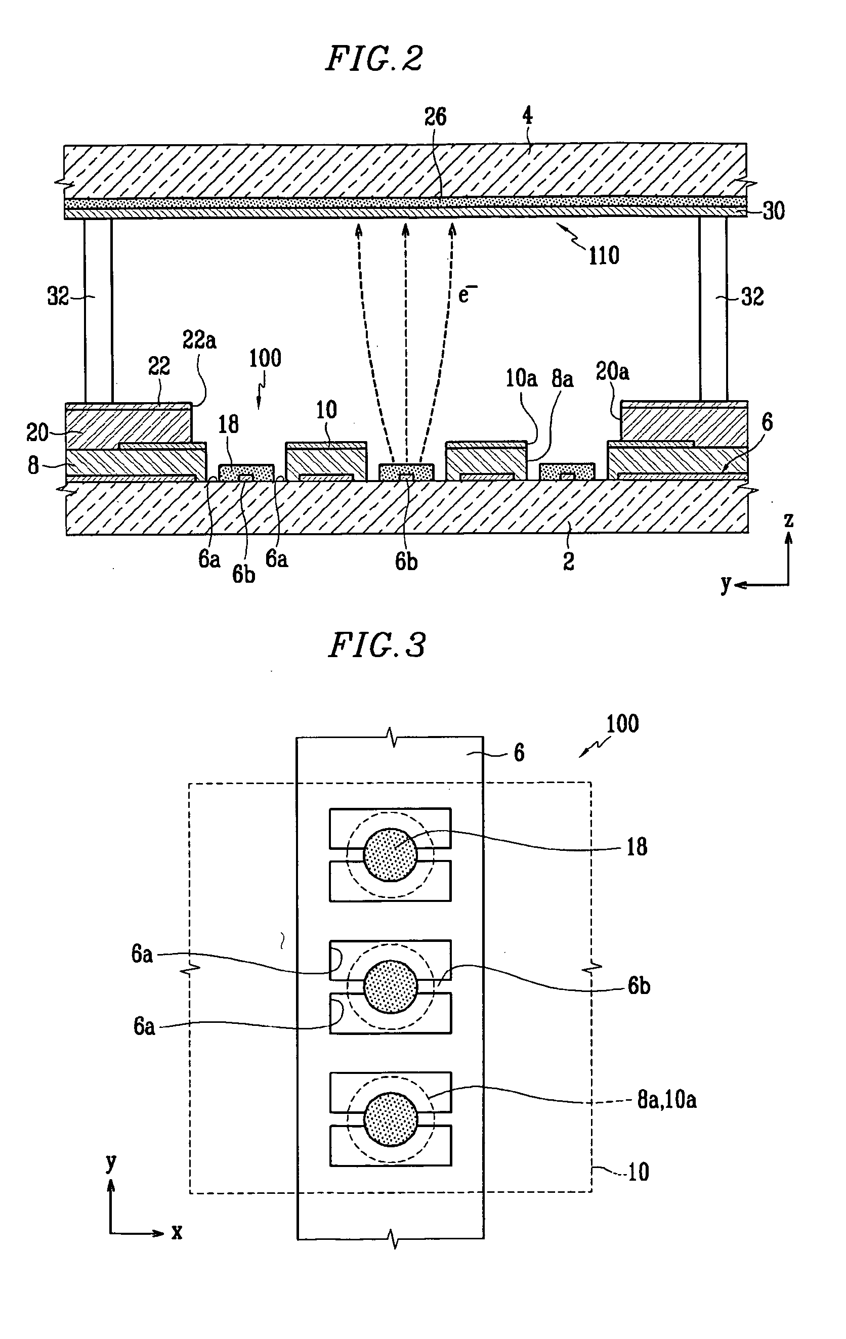
[0032]FIGS. 1A-3 illustrate exploded, sectional and plan views, respectively, of an electron emission display according to the present invention. Referring to FIGS. 1A-3, the electron emission display may include an electron emission device 100 and a light emission device 110. The electron emission device 100 and the light emission device 110 may include first and second substrates 2 and 4, respectively. The first and second substrates 2 and 4 may be joined and sealed with a sealing member (not shown) provided at the peripheries of the first and the second substrates 2 and 4, thereby forming a sealed vacuum vessel.

[0033] The electron emission device 100 may include an array of electron emission elements formed on a surface of the first substrate 2 that faces the second substrate 4. In detail, cathode electrodes 6 may be arranged on the first substrate 2, e.g., in a striped pattern, and a first insulating layer 8 may formed on the first substrate 2 to fully cover the cathode electrod...

fourth embodiment

[0067] Similar to the electron emission region 18′ of FIG. 9, the electron emission region 18″ of the fourth embodiment may have an increased effective length of the edges where electron mission intensively occurs, as a result of the multiple portions making up the electron emission region 18″. Thus, electron emission efficiency may be further enhanced. In addition, since the electric field may be effectively concentrated on the top edges of the portions of the electron emission region 18″ that face the bridge members 6b′, the emission efficiency may be further enhanced.

[0068] A method of forming electron emission regions for the above-described embodiments will now be explained with reference to FIGS. 11A-11C and 11C (ALT.), which illustrate partial sectional views of stages in a method of making an electron emission device according to the present invention.

[0069] Referring to FIG. 11A, the cathode electrodes 6, the first insulating layer 8, the gate electrodes 10, the second ins...


PUM


Abstract

An electron emission device includes a first electrode disposed on a substrate, an electron emission region electrically coupled to the first electrode, and a second electrode spaced apart from the first electrode, wherein the first electrode includes an opening and an extension that projects into the opening, and the electron emission region is electrically coupled to the first electrode by the extension.

Description

BACKGROUND OF THE INVENTION [0001] 1. Field of the Invention [0002] The present invention relates to an electron emission device and an electron emission display using the electron emission device. More particularly, the present invention relates to an electron emission device configured to enhance electron emission efficiency and an electron emission display using the same. [0003] 2. Description of the Related Art [0004] Generally, electron emission devices may be classified according to whether a hot cathode technology or a cold cathode technology is employed to generate electron emission. There are several types of cold cathode-based electron emission devices including, e.g., Field Emission Array (FEA) devices, Surface-Conduction Emission (SCE) devices, Metal-Insulator-Metal (MIM) devices and Metal-Insulator-Semiconductor (MIS) devices. [0005] The FEA devices typically include electron emission regions, and cathode and gate electrodes as driving electrodes. The electron emission ...

Claims


Application Information

Patent Timeline
IPC IPC(8): H01J1/62H01J63/04
CPCH01J31/127H01J1/304H01J2201/30453H01J2201/30469
Inventor HWANG, SEONG-YEONLEE, SEUNG-HYUN
Owner SAMSUNG SDI CO LTD
Learn More