
Method for suppressing anti-short channel effect and method for manufacturing nmos device

A short-channel effect and device technology, applied in semiconductor/solid-state device manufacturing, semiconductor devices, electrical components, etc., can solve the problems of difficulty in further suppressing the RSCE effect, small IO size, etc., and achieve the effect of suppressing the anti-short-channel effect.

Active Publication Date: 2018-06-22
SHANGHAI HUALI MICROELECTRONICS CORP
View PDF5 Cites 0 Cited by
  • Summary
  • Abstract
  • Description
  • Claims
  • Application Information

AI Technical Summary

Problems solved by technology

However, when the technology node is below 90nm, the IO size is very small, and it is difficult to further suppress the RSCE effect only by optimizing the annealing process.

Method used


Image

  • Method for suppressing anti-short channel effect and method for manufacturing nmos device
  • Method for suppressing anti-short channel effect and method for manufacturing nmos device
  • Method for suppressing anti-short channel effect and method for manufacturing nmos device

Examples


Embodiment Construction

[0040] In order to make the content of the present invention clearer and easier to understand, the content of the present invention will be further described below in conjunction with the accompanying drawings. Of course, the present invention is not limited to this specific embodiment, and general replacements known to those skilled in the art are also covered within the protection scope of the present invention.

[0041] The following is attached Figure 3-10 The method for suppressing the reverse short channel effect of an NMOS device of the present invention will be further described in detail with specific embodiments. It should be noted that the drawings are all in a very simplified form, using imprecise scales, and are only used to facilitate and clearly achieve the purpose of assisting in describing the present embodiment.

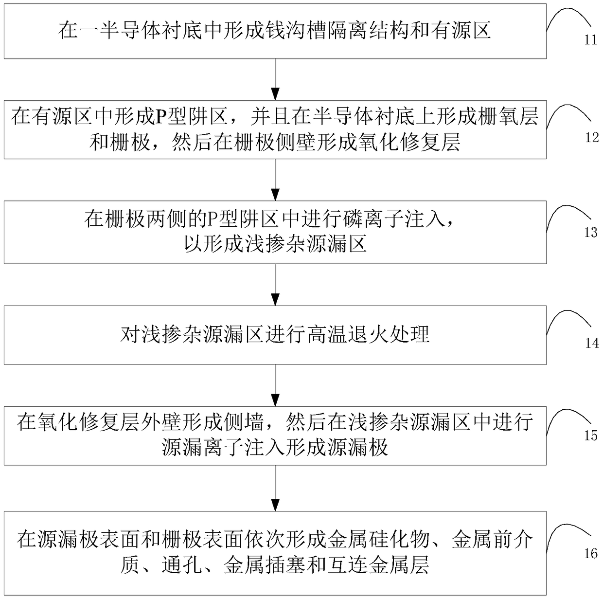
[0042] see image 3 , the method for suppressing the reverse short channel effect of the NMOS device of the present embodiment comprises the fol...


PUM


Abstract

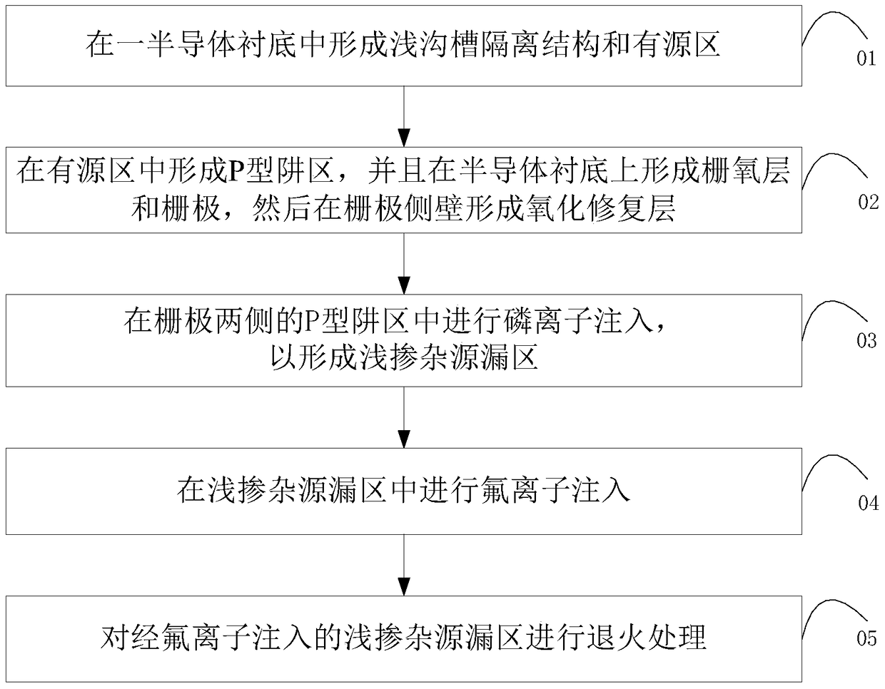
The invention provides a method for restraining the reverse short channel effect and a manufacturing method of an NMOS (N-Channel Metal Oxide Semiconductor) device. After phosphorus ions are injected into the drain region of a shallow doping source, a fluorine ion injection procedure is added, and low-temperature annealing long-time treatment is performed on the drain region of the shallow doping source. The injected fluorine ions are combined with vacancy and interstitial atoms and the like in a grid edge area, so that the diffusion of boron elements in a P-type well region can be prevented, and the reverse short channel effect is restrained. Moreover, the fluorine ions can restrain hot carrier injection, so that the reliability of hot carrier injection does not become poor while the fluorine ions are injected.

Description

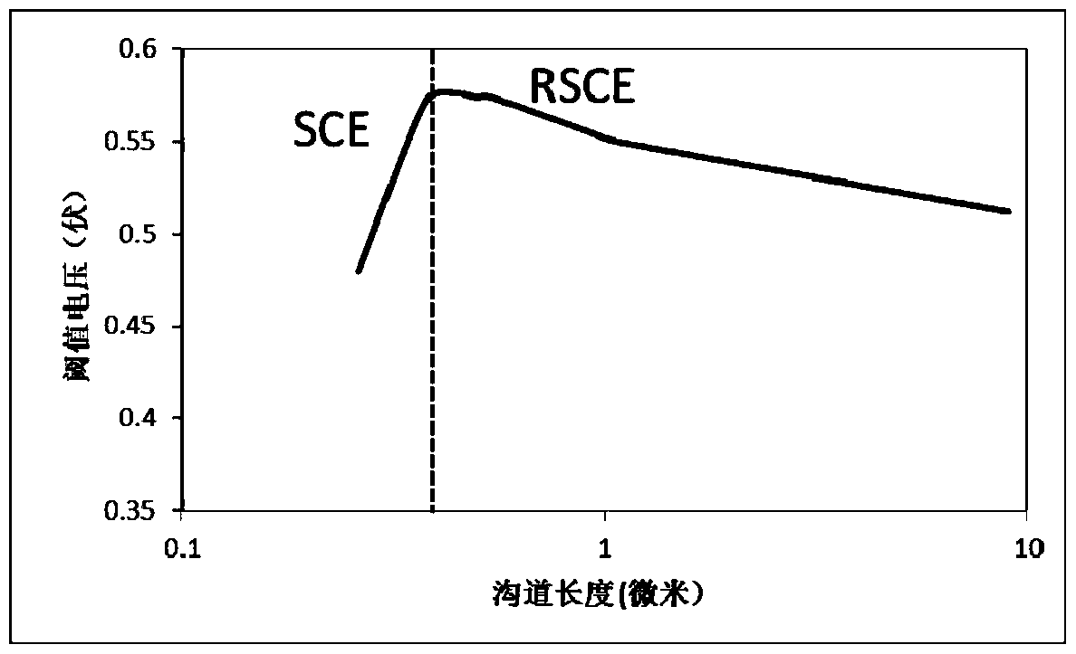
technical field [0001] The invention relates to the technical field of semiconductors, in particular to a forming method for suppressing the anti-short channel effect of an NMOS device and a preparation method of the NMOS device. Background technique [0002] With the rapid development of VLSI technology, the size of MOSFET devices is constantly decreasing. As the channel length decreases, the threshold voltage of MOSFET devices will first increase, and when the channel length is further reduced, the threshold voltage will decrease again. ,Such as figure 1 As shown, it is a schematic diagram of the curve of the channel length of the existing NMOS device changing with the threshold voltage; what is behind the dotted line is called the short channel effect (short channel effect, hereinafter referred to as SCE), and what is in front of the dotted line is called the reverse short channel effect. (reverse short channel effect, hereinafter referred to as RSCE), usually the RSCE e...

Claims


Application Information

Patent Timeline
Patent Type & Authority Patents(China)
IPC IPC(8): H01L21/336H01L21/265
CPCH01L21/265H01L29/66477
Inventor 卢海峰刘巍
Owner SHANGHAI HUALI MICROELECTRONICS CORP
Learn More