Optical waveguide chip coupling test fixture

A technology for testing fixtures and chip fixtures, applied in the field of optical waveguides, can solve the problems of lack of adjustment function, limited application scope, single fixing method of fixture chips, etc., and achieves flexible chip attitude adjustment, wide application range, and optimized coupling adjustment effect. Effect

Active Publication Date: 2018-02-09
SHENZHEN GRADUATE SCHOOL TSINGHUA UNIV
View PDF8 Cites 0 Cited by
  • Summary
  • Abstract
  • Description
  • Claims
  • Application Information

AI Technical Summary

Problems solved by technology

Most of the existing optical waveguide chip fixtures are customized according to the specific chip to be coupled. This type of fixture can only be used for optical waveguide chips of a specific size and shape, so the application range is limited, and the chip fixing method of this type of fixture is often relatively simple. At the same time It also lacks the adjustment function to adapt to different application environments

Method used


Image

  • Optical waveguide chip coupling test fixture
  • Optical waveguide chip coupling test fixture
  • Optical waveguide chip coupling test fixture

Examples


example 1

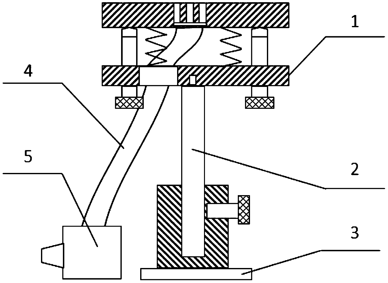
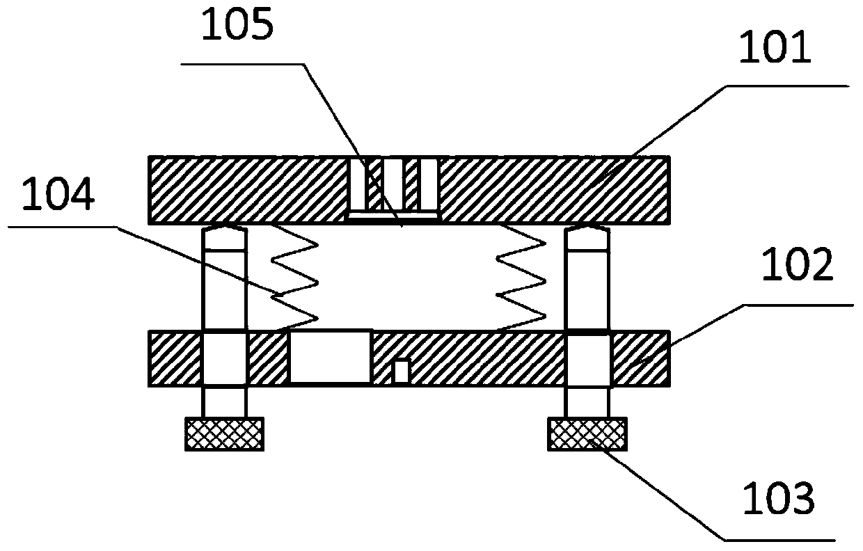
[0039] Aluminum alloy is selected as the manufacturing material of the film holder, stainless steel is selected as the manufacturing material of the support rod and the support seat, rubber is used to make the air guide hose, and standard parts such as the height adjustment screw and the inclination angle adjustment screw are selected.

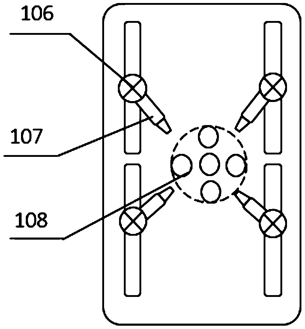
[0040] The film holder is designed to be 8cm in length, 4cm in width, and 3cm in height, the aperture of the suction piece is 3mm, and the entire area of ​​the suction piece is 1cm 2 , the support rod is 12cm long, the entire optical waveguide chip coupling test fixture can be adjusted in height from 16 to 21cm, and the tilt and pitch adjustment angle of the wafer stage is -5° to 5°.

[0041] The optical waveguide chip coupling test fixture shown in the above example can be used for clamping the optical waveguide chip and adjusting the chip height and tilt angle in the optical fiber optical waveguide chip coupling test.


PUM


Abstract

An optical waveguide chip coupling test fixture, comprising a wafer table and a supporting structure for supporting the wafer table, a chip holder is arranged on the wafer table, and the chip holder includes a plurality of chip fixing adjustment knobs and connecting Chip fixing clips on each of the chip fixing adjustment knobs, a plurality of the chip fixing clips are arranged in a form that surrounds the chip to be fixed in the central area, and the chip fixing clips can be adjusted by each chip fixing adjustment knob The fixed position and fixed angle of the chip. The invention can be used for the clamping and fixing of the optical waveguide chip and the adjustment of the fixing angle of the optical waveguide chip for the end face coupling of the optical fiber and the optical waveguide, and is suitable for optical waveguide chips of various shapes and sizes. It has the advantages of flexible posture adjustment, easy disassembly and replacement of the chip held, simple and convenient operation, and wide application range.

Description

technical field [0001] The invention relates to the field of optical waveguide technology, in particular to an optical waveguide chip coupling test fixture, which is used for clamping and fixing the optical waveguide chip and adjusting the height, tilt and pitch angle of the optical waveguide chip when the optical fiber is coupled with the end face of the optical waveguide. Background technique [0002] Entering the 21st century, with the upgrading of computer technology and the rise of the information industry, the wave of information revolution has entered a new stage. Human beings are moving from the Internet where everyone is connected to the Internet where everything is connected. Information age of big data. People have a higher demand for information transmission speed, which brings new challenges to the existing network system, the bandwidth, reliability, confidentiality and low power consumption of integrated circuit chips, and the concept of all-optical network thu...

Claims


Application Information

Patent Timeline
Patent Type & Authority Patents(China)
IPC IPC(8): G01M11/00
Inventor 董瑛刘渝进
Owner SHENZHEN GRADUATE SCHOOL TSINGHUA UNIV
Why Eureka
Try Eureka