Three-state metal oxide semiconductor thin film transistor and its preparation method

A technology of oxide semiconductor and thin film transistor, applied in semiconductor/solid-state device manufacturing, transistors, semiconductor devices, etc., can solve problems such as low sensitivity to visible light

Active Publication Date: 2019-01-11
PEKING UNIV
View PDF3 Cites 0 Cited by
  • Summary
  • Abstract
  • Description
  • Claims
  • Application Information

AI Technical Summary

Problems solved by technology

4. Oxide materials are difficult to generate photogenerated carriers under light irradiation, and have low sensitivity to visible light

Method used


Image

  • Three-state metal oxide semiconductor thin film transistor and its preparation method
  • Three-state metal oxide semiconductor thin film transistor and its preparation method
  • Three-state metal oxide semiconductor thin film transistor and its preparation method

Examples


Embodiment Construction

[0026] The present invention will be further described below by example. It should be noted that the purpose of the disclosed examples is to help further understand the present invention, but those skilled in the art can understand that various replacements and modifications are possible without departing from the scope of the present invention and the spirit of the appended claims. Therefore, the present invention should not be limited to the content disclosed in the examples, and the protection scope of the present invention is subject to the scope defined in the claims.

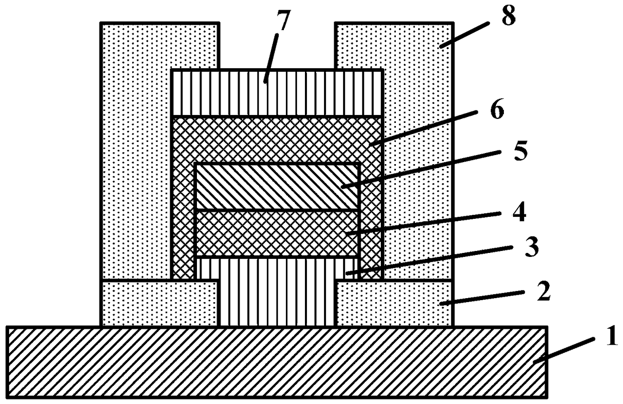
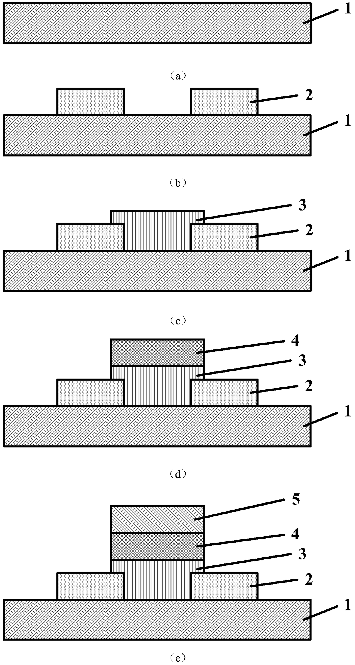
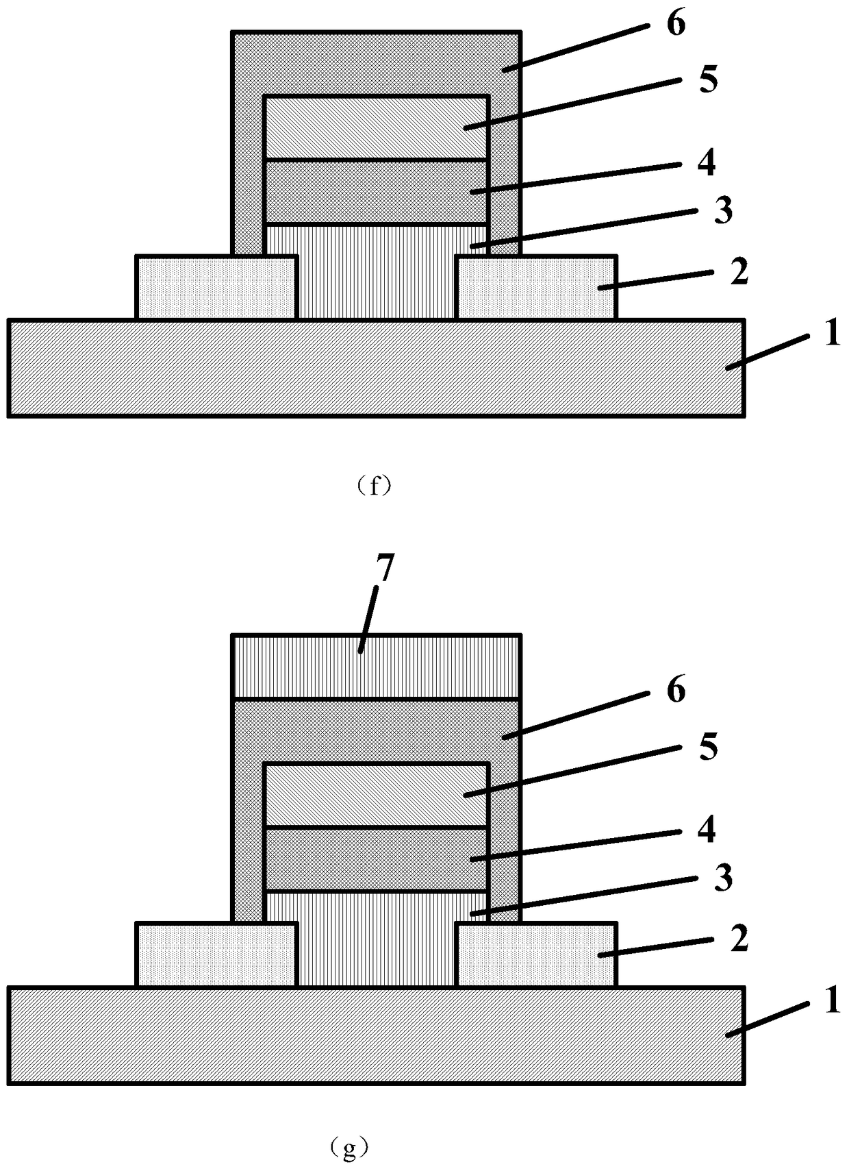
[0027] The tri-state metal oxide semiconductor thin film transistor of the present invention is formed on a glass or plastic substrate, such as figure 1 shown. The tri-state metal oxide semiconductor thin film transistor comprises a bottom source and drain electrode, a bottom channel, a bottom gate dielectric, a gate electrode, a top gate dielectric, a top channel layer, and a top source and drain electro...


PUM


Abstract

The invention provides a tristate metal oxide semiconductor thin film transistor and a preparation method thereof, which belongs to the field of flat panel display in the semiconductor industry. The tristate metal oxide semiconductor thin film transistor sequentially comprises a substrate, a bottom-layer source-drain electrode, a bottom-layer channel layer, a bottom-layer gate dielectric layer, a gate electrode, a top-layer gate dielectric layer, a top-layer channel layer and a top-layer source-drain electrode from bottom to top, wherein the thickness of the top-layer gate dielectric is larger than that of the bottom-layer gate dielectric, or the top-layer gate dielectric has a smaller dielectric constant than the bottom-layer gate dielectric; and conductivity of the top-layer channel material is better than that of the bottom-layer channel material. As a top gate structure and a bottom gate structure are overlapped to form the structure, transfer characteristics are overlapping of transfer characteristics of the upper device and the lower device, and performance of the traditional metal oxide semiconductor thin film transistor is broken.

Description

technical field [0001] The invention relates to a method for preparing a semiconductor thin film transistor on a glass substrate or a plastic substrate, belonging to the field of semiconductor industry and flat panel display. Background technique [0002] The 21st century is an era of informatization, and display technology is also developing rapidly. CRT displays, PDP displays, LCD displays, OLED displays, etc. have been born successively. These flat panel displays have been improved in brightness, contrast, color, power consumption and volume Overall improvement. Research on new display technologies has always been a research hotspot in the field of flat panel displays, including transparent display, flexible display, and naked-eye 3D display technologies that have received widespread attention. [0003] Silicon-based materials can no longer meet the needs of new display technologies due to their sensitivity to light and poor stability. Although Poly-Si TFT has high mobi...

Claims


Application Information

Patent Timeline
Patent Type & Authority Patents(China)
IPC IPC(8): H01L29/786H01L29/423H01L29/06H01L21/34
CPCH01L29/0684H01L29/42364H01L29/42368H01L29/42384H01L29/66969H01L29/7869
Inventor 韩德栋郁文王漪石盼张翼黄伶灵丛瑛瑛董俊辰张盛东刘晓彦康晋锋
Owner PEKING UNIV
Why Eureka
Try Eureka