

A Double Heterojunction Pin Electro-optic Modulator Structure
An electro-optical modulator and double heterojunction technology, which is applied in the fields of instruments, optics, nonlinear optics, etc., can solve the problem of increasing the modulation power consumption of devices, and achieve the goal of reducing optical transmission loss, facilitating optoelectronic integration, and reducing modulation power consumption. Effect
- Summary
- Abstract
- Description
- Claims
- Application Information
AI Technical Summary
Problems solved by technology
Method used
Image

Examples
Embodiment Construction
[0023] The present invention will be described in detail below with reference to the accompanying drawings and specific embodiments.
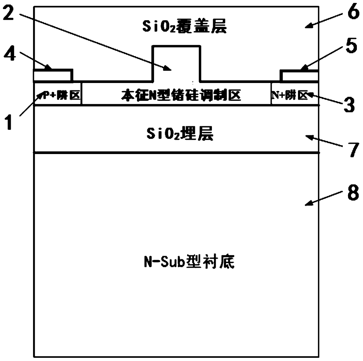
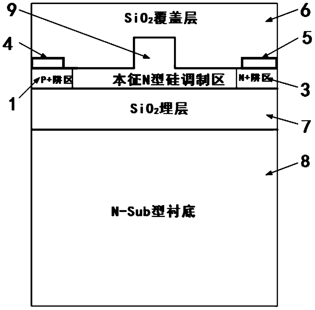
[0024] The present invention is a double heterojunction PIN electro-optic modulator structure, such as figure 1 As shown, an N-Sub type substrate 8 is included, and the upper part of the N-Sub type substrate 8 is provided with SiO 2 Buried Layer 7, SiO 2 A P+ well region 1 and an N+ well region 3 are respectively provided on both sides of the upper part of the buried layer 7, an intrinsic N-type silicon germanium modulation region 2 is provided between the P+ well region 1 and the N+ well region 3, and the upper part of the P+ well region 1 is provided There is a first electrode 4, the upper part of the N+ well region 3 is provided with a second electrode 5, and the upper part of the first electrode 4, the intrinsic N-type germanium-silicon modulation region 2 and the second electrode 5 is covered with SiO 2 cover layer 6.
[0025] The struc...
PUM
| Property | Measurement | Unit |
|---|---|---|
| height | aaaaa | aaaaa |
| width | aaaaa | aaaaa |
| width | aaaaa | aaaaa |
Abstract
Description
Claims
Application Information