
A kind of preparation method of mos transistor

A MOS transistor and region technology, applied in semiconductor/solid-state device manufacturing, semiconductor devices, electrical components, etc., can solve the problems of limited breakdown voltage, etc., and achieve the goal of increasing operating current, improving short channel effect, and increasing implant concentration Effect

Active Publication Date: 2017-10-20
SEMICON MFG INT (SHANGHAI) CORP
View PDF4 Cites 0 Cited by
  • Summary
  • Abstract
  • Description
  • Claims
  • Application Information

AI Technical Summary

Problems solved by technology

[0010] On the other hand, in the prior art, ion implantation is usually used to form different doping distributions, so as to achieve the purpose of changing the breakdown voltage of the transistor, so that the transistor can be used in ESD electrostatic discharge protection. However, the adjusted The breakdown voltage is limited, and the existing technology has not improved the essential structure of the device

Method used


Image

  • A kind of preparation method of mos transistor
  • A kind of preparation method of mos transistor
  • A kind of preparation method of mos transistor

Examples


Embodiment Construction

[0047] Embodiments of the present invention are described below through specific examples, and those skilled in the art can easily understand other advantages and effects of the present invention from the content disclosed in this specification. The present invention can also be implemented or applied through other different specific embodiments, and various modifications or changes can be made to the details in this specification based on different viewpoints and applications without departing from the spirit of the present invention.

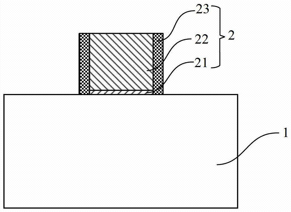
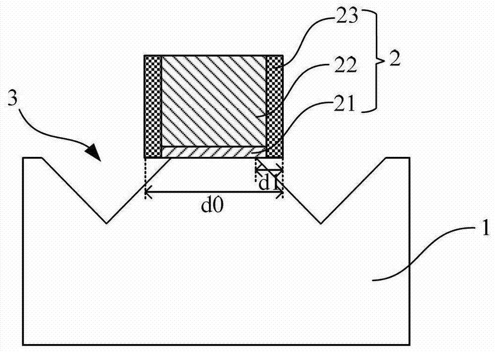
[0048] see Figure 2 to Figure 9 . It should be noted that the illustrations provided in the following specific embodiments are only schematically illustrating the basic idea of ​​the present invention, and only the components related to the present invention are shown in the drawings rather than the number and shape of components in actual implementation. and size drawing, the type, quantity and proportion of each component can be changed ar...


PUM


Abstract

The invention provides a preparation method of a MOS transistor. During preparation of a source region and a drain region, a V-shaped groove is first of all etched by use of a wet method, afterwards, a stress filling layer is grown in an epitaxial mode in the V-shaped groove, a lightly doped area is formed in the stress filling layer near a gate area, and finally, the source region and the drain region are formed through ion implantation. Compared to horizontal-W-shaped source and drain regions in the prior art, the stress filling layer is formed by filling the V-shaped groove and is taken as the source region and the drain region, so that the source region and the drain region are closer to a channel, and the stress effects which the source region and the drain region apply to the channel are more obvious; a heterojunction is formed at the bottom of the stress filling layer in the V-shaped groove so that there are much tip-end electric leakage at the bottom of the stress filling layer, and the application of the method in the aspect of ESD electrostatic discharge is improved in terms of structure; and the source region and the drain region formed by filling the V-shaped groove are quite far away from each other, so that the effective channel length is increased, the short channel effect is improved, and the working currents are improved.

Description

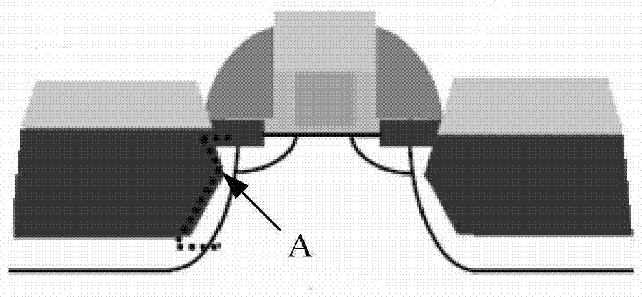
technical field [0001] The invention belongs to the technical field of semiconductor devices and relates to a preparation method of a MOS transistor. Background technique [0002] With the development of semiconductor technology, the feature size of devices in integrated circuits is getting smaller and smaller. When the manufacturing process of CMOS progresses to the micron level, the channel between the source / drain regions becomes shorter. When the length of the channel region is reduced to a certain value, a short channel will be generated. Channel Effect (Short Channel Effect) and Hot Carrier Effect (Hot Carrier Effect) and thus cause the device to fail to operate. In other words, since the existence of the short channel effect will affect the performance of the device, it also hinders the further reduction of the feature size of the device in the integrated circuit. [0003] In order to avoid short-channel effects and hot-carrier effects, the source / drain design of CM...

Claims


Application Information

Patent Timeline
Patent Type & Authority Patents(China)
IPC IPC(8): H01L21/336
CPCH01L29/66636H01L29/7848
Inventor 赵猛
Owner SEMICON MFG INT (SHANGHAI) CORP
Learn More