Developing device and photolithography equipment

A developing device and photoresist technology, which is applied in the processing of photosensitive materials, can solve the problems of open circuit, scratching, and affecting product quality, so as to improve the development speed, prevent the disconnection of the active layer, and improve the uniformity of development.

Inactive Publication Date: 2019-09-17
BOE TECH GRP CO LTD +1
View PDF7 Cites 0 Cited by
  • Summary
  • Abstract
  • Description
  • Claims
  • Application Information

AI Technical Summary

Problems solved by technology

The different development speeds lead to different degrees of dissolution of the photoresist, resulting in different thicknesses of the photoresist in different regions. When the thickness of the photoresist is too high, after the second etching, the source and drain are connected together to make the thin film transistor A short circuit occurs. When the thickness of the photoresist is too low, it is easy to cause the active layer to be cut through and an open circuit occurs, thus affecting the quality of the product

Method used


Image

  • Developing device and photolithography equipment
  • Developing device and photolithography equipment
  • Developing device and photolithography equipment

Examples


Embodiment approach

[0034] As another specific embodiment of the present invention, the control mechanism can control the opening state and / or heating temperature of each heating member 21 according to the development speed of each development position on the substrate when the substrate is not heated, so that During the developing process, the developing speeds of the plurality of developing positions on the substrate 30 are the same.

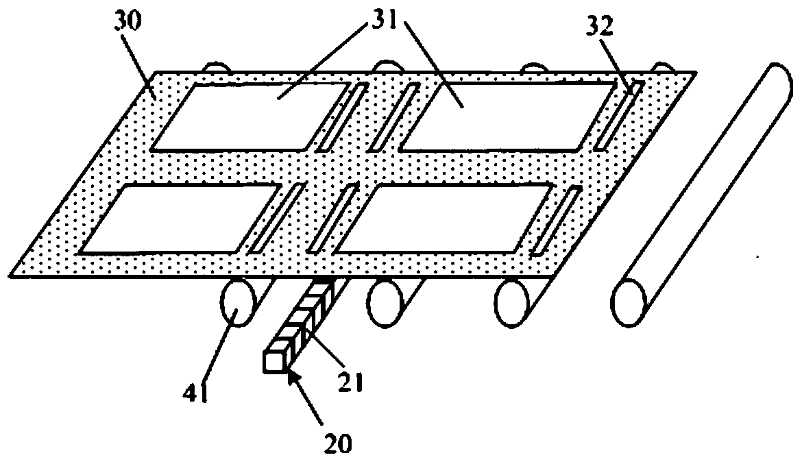
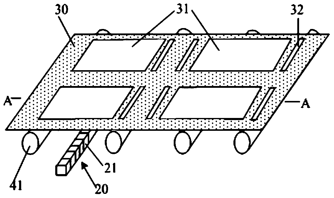
[0035] Such as figure 2 , image 3 and Figure 6As shown, the substrate 30 includes a display area 31 and a driving area 32 for setting a gate driving circuit around the display area. In order to make the developing speeds of the display area 31 and the non-display area consistent, the heating mechanism may include two independently controlled heating elements, which are respectively used to heat the display area and the periphery of the display area of ​​the substrate above the heating mechanism. The drive zone is heated, and the control mechanism can contro...


PUM


Abstract

The invention discloses a developing device and photoetching equipment. The developing device comprises developing chambers, wherein the developing chambers are used for accommodating to-be-developed substrates; the developing device further comprises a heating mechanism; the heating mechanism comprises a plurality of heating pieces, and the plurality of heating pieces are arranged in the developing chambers, are used for heating different developing positions of the substrates, located above or below the heating mechanism, in the developing chambers and can independently control heating respectively.

Description

technical field [0001] The invention relates to the technical field of display panel production, in particular to a developing device and photolithography equipment. Background technique [0002] Fabrication of the array substrate usually uses a 1+4mask process, and the active layer, source level, and drain are formed through a photolithography patterning process. Specifically, firstly, a semiconductor layer, a source-drain material layer, and a photoresist layer are sequentially formed; secondly, a semi-transparent mask is used to expose and develop the photoresist, so that the thickness of the photoresist corresponding to the channel region after development is smaller than that of the corresponding channel region. The photoresist thickness of the source and drain electrodes, while the photoresist at the rest of the position is dissolved by the developer; then the first etching is performed to form the active layer pattern and the connected source and drain electrodes; aft...

Claims


Application Information

Patent Timeline
Patent Type & Authority Patents(China)
IPC IPC(8): G03F7/30
Inventor 刘明悬陈曦张小祥郭会斌袁剑峰孙增标罗丽平刘会双闵苏
Owner BOE TECH GRP CO LTD
Why Eureka
Try Eureka