Automatic optics testing device and method for PCBs

A PCB board and automatic optical technology, applied in the field of PCB automatic optical inspection device, can solve problems such as low efficiency of operation, scratches on PCB board lines, and hidden quality problems, and achieve the effect of high board separation efficiency

Inactive Publication Date: 2015-12-09
HUANGSHI HUSHI ELECTRONICS CO LTD
View PDF7 Cites 5 Cited by
  • Summary
  • Abstract
  • Description
  • Claims
  • Application Information

AI Technical Summary

Problems solved by technology

However, the existing technology has the following defects: a. The efficiency of the operation method is low; b. There are hidden dangers in quality, which may easily cause scratches on the circuit of the PCB board

Method used


Image

  • Automatic optics testing device and method for PCBs

Examples


Embodiment Construction

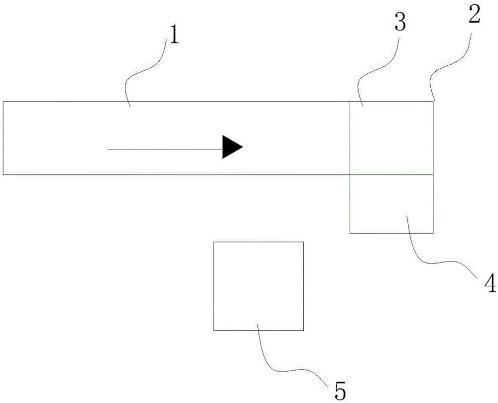
[0016] Such as figure 1 As shown, an automatic optical inspection device for PCB boards includes a conveying acceleration section 1 , a steering angle temporary storage machine 2 , a conveying storage position 4 , a sensor 3 , and an AOI device 5 .

[0017] The steering angle temporary storage machine 2 is set at the conveying end of the conveying acceleration section 1; the sensor 3 is set inside the steering angle temporary storage machine 2; the conveying storage position 4 is set on the side of the steering angle temporary register; the AOI equipment 5 is set at the conveying storage next to bit 4. figure 1 The direction of the middle arrow is the direction of PCB board transmission.

[0018] Optionally, the AOI equipment 5 and the delivery storage position 4 are located on the same side relative to the steering angle temporary register.

[0019] Optionally, in the automatic optical inspection device for PCB boards according to the embodiment of the present invention, th...


PUM


Abstract

The invention provides an automatic optics testing device and method for PCBs. The automatic optics testing device comprises a conveying acceleration section, a steering corner temporary storage machine, a conveying storage position, an inductor and AOI equipment. The steering corner temporary storage machine is arranged at the conveying tail end of the conveying acceleration section. The inductor is arranged at the inner side of the steering corner temporary storage machine. The conveying storage position is arranged at one side of the steering corner temporary storage machine. The AOI equipment is arranged beside the conveying storage position. The invention further provides an automatic optics testing method for the PCBs. The method is implemented through the automatic optics testing device for the PCBs. The method comprises the following steps that 1, the PCBs are sequentially conveyed to the conveying acceleration section after being treated through a copper etching technology; 2, whether the PCBs reach the steering corner temporary storage machine is judged by means of the inductor, and when the PCBs reach the steering corner temporary storage machine, the steering corner temporary storage machine enables the PCBs to be steered and conveys the PCBs into the conveying storage position; the PCBs in the conveying storage position are conveyed into the AOI equipment; automatic optics testing is carried out on the PCBs by means of the AOI equipment.

Description

technical field [0001] The invention relates to the technical field of inspection in the production process of PCB boards, in particular to an automatic optical inspection device and method for PCB boards. Background technique [0002] In the production process of printed circuit boards (PCB boards), after the etching copper process (Developing / Etching / Stripping; DES) of the inner layer (InnerLayer) of the PCB board is completed, the boards are divided manually, and then the automatic optical inspection (AutomaticOpticInspection; Test the defect category and location on the AOI) equipment, and then check the defects on the defect detection confirmation and repair equipment (Verified&Repaired; VRS). However, the prior art has the following defects: a. low operating efficiency; b. hidden quality problems, which can easily cause scratches on the circuit of the PCB board. Contents of the invention [0003] In view of this, the present invention provides an automatic optical i...

Claims


Application Information

Patent Timeline
Patent Type & Authority Applications(China)
IPC IPC(8): B65G47/88B65G47/24G01N21/88
Inventor 张文和
Owner HUANGSHI HUSHI ELECTRONICS CO LTD
Why Eureka
Try Eureka