Eureka AIR delivers breakthrough ideas for toughest innovation challenges, trusted by R&D personnel around the world.

Clock circuit for FPGA verification platform

A technology of clock circuit and verification platform, applied in the direction of electrical components, automatic power control, generation/distribution of signals, etc., can solve the problems of high hardware cost and labor cost, different clock frequency, long development time, etc., to reduce hardware cost and manpower cost, the effect of shortening the development time

Active Publication Date: 2015-12-09
FENGHUO COMM SCI & TECH CO LTD
View PDF5 Cites 2 Cited by
  • Summary
  • Abstract
  • Description
  • Claims
  • Application Information

AI Technical Summary

Problems solved by technology

[0009] The technical problem to be solved by the present invention is to solve the problem that due to the different speeds of various PON systems, the required clock frequencies are also different, resulting in high hardware costs and labor costs in technology development, and it takes a long time to develop.

Method used


Image

  • Clock circuit for FPGA verification platform

Examples


Embodiment Construction

[0020] The present invention will be described in detail below in conjunction with the accompanying drawings and specific embodiments.

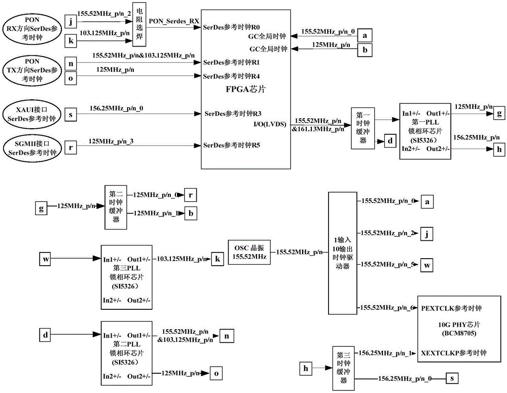
[0021] The embodiment of the present invention provides a clock circuit for an FPGA verification platform. The FPGA verification platform can verify four different PON systems: XG-PON system, symmetrical 10GEPON system, asymmetrical 10GEPON system and GPON system only through the FPGA chip , the block diagram of the clock circuit is shown in figure 1 shown.

[0022] From the uplink and downlink rates of the four PON systems listed in the background technology, the downlink rates have three different rate levels, namely 9.95328Gbit / s (XG-PON system), 10.3125Gbit / s (symmetrical 10GEPON and asymmetrical 10GEPON systems) ) and 2.48832Gbit / s (GPON system), but there is an obvious multiple relationship between 9.95328Gbit / s and 2.48832Gbit / s, so two different SerDes (SERializer / DESerializer, serializer) in the downlink direction of the PON port ar...


PUM


Abstract

The invention discloses a clock circuit for an FPGA verification platform. The clock circuit comprises an FPGA and a 10G PHY chip, and further comprises clock buffers and a clock driver; a line recovery clock is divided into two parts through the first clock buffer, one part is converted into a clock g and a clock h through a first PLL, and the other part is a clock d; the clock d is converted into a reference clock in the uplink direction of a PON port through a second PLL; the clock g is divided into a clock r and a clock b through the second clock buffer; the clock r is a reference clock of an SGMII; the clock b is a reference clock of the FPGA; the clock h is divided into a reference clock (XEXTCLK) and a clock s; the clock s is a reference clock of an XAUI; a PON logic clock a, a reference clock j in the downlink direction of the PON port, a clock w and a reference clock (PEXTCLK) are all provided by a clock driver; the clock w is converted into a reference clock k in the downlink direction of the PON port through a third PLL. Through adoption of the clock circuit, the hardware and human costs during technical development are remarkably reduced, and the development period is effectively shortened.

Description

technical field [0001] The invention relates to the field of clock circuits, in particular to a clock circuit used for an FPGA verification platform. Background technique [0002] PON (PassiveOpticalNetwork, Passive Optical Network) system is mainly composed of OLT (OpticalLineTerminal, Optical Line Terminal), ONU (OpticalNetworkUnit, Optical Network Unit) and ODN (OpticalDistributionNetwork, Optical Distribution Network), usually using a point-to-multipoint tree topology structure. The most common PON systems are: XG-PON (10-Gigabit-capablePassiveOpticalNetwork, 10 Gigabit Ethernet Passive Optical Network) system, 10GEPON (EthernetPassiveOpticalNetwork, Ethernet Passive Optical Network) system and GPON (Gigabit-CapablePON, gigabit Ethernet passive optical network) system. [0003] For the XG-PON system, the uplink and downlink rate parameters are defined as follows: 9.95328Gbit / s downlink, 2.48832Gbit / s uplink. [0004] For the 10GEPON system, the uplink and downlink rat...

Claims


Application Information

Patent Timeline
IPC IPC(8): G06F1/08H03L7/08
Inventor 黄元波李恒
Owner FENGHUO COMM SCI & TECH CO LTD
Why Eureka
Eureka Blog
Learn More