Electromagnetic shielding encapsulation method and encapsulation structure

A technology of electromagnetic shielding and packaging method, applied in the direction of circuits, electrical components, electrical solid devices, etc., can solve the problems of high integration, product reliability and performance impact, and void phenomenon

Active Publication Date: 2015-12-09
JCET GROUP CO LTD
View PDF9 Cites 6 Cited by
  • Summary
  • Abstract
  • Description
  • Claims
  • Application Information

AI Technical Summary

Problems solved by technology

[0004] 1. Due to the large number of electronic devices mounted on the substrate, the integration is high, the distance between the devices is small, and the encapsulation area is large, the phenomenon of backpacking is more obvious, and it is easy to cause voids during the encapsulation process, which in turn affects the reliability of the product. have a certain impact;
[0005] 2. Because the traditional process uses laser slotting, it has high requirements for laser precision, and a slight deviation is easy to damage the device. The laser energy also needs to be controlled within an appropriate range, otherwise it will cause different degrees of damage to the substrate

Method used


Image

  • Electromagnetic shielding encapsulation method and encapsulation structure
  • Electromagnetic shielding encapsulation method and encapsulation structure
  • Electromagnetic shielding encapsulation method and encapsulation structure

Examples


Embodiment Construction

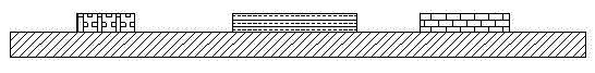
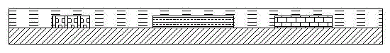
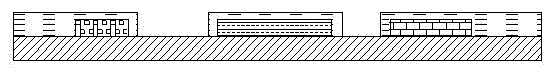
[0038] see Figure 7 , an electromagnetic shielding packaging structure of the present invention, it includes a substrate 1, a radio frequency chip 2, a first electronic device 3 and a second electronic device 4 are mounted on the front of the substrate 1, the radio frequency chip 2, the first electronic device 3 And the second electronic device 4 is covered with a layer of dry film 5, the dry film 5 area around the radio frequency chip 2 is opened with a filling groove 6 through exposure and development, and the filling material 6 is filled with metal fillers 7, the metal fillers The upper surface of 7 is flush with the upper surface of dry film 5, and a layer of metal layer 8 is sputtered on the upper surfaces of dry film 5 and metal filler 7, and the metal filler 7 and sputtered metal layer 8 form an electromagnetic shielding structure.

[0039] The metal filler 7 can be replaced by liquid copper or thin metal film.

[0040] Its process method is as follows:

[0041] Step...


PUM


Abstract

The invention relates to an electromagnetic shielding encapsulation method and encapsulation structure. The structure comprises a substrate (1); a radio frequency chip (2) and a plurality of electronic devices are arranged on the front surface of the substrate (1) through surface mount technology; the radio frequency chip (2) and the plurality of electronic devices are covered with a dry film (5); filling grooves (6) located at the peripheries of the radio frequency chip (2) and the plurality of electronic devices are formed at the dry film (5) through exposure development; metal fillers (7) are arranged in the filling grooves (6); and the upper surfaces of the dry film (5) and the metal fillers (7) are provided with a metal layer (8). With the electromagnetic shielding encapsulation method and the encapsulation structure of the invention adopted, the problems of defects existing in encapsulation and laser slotting in traditional technologies can be solved.

Description

technical field [0001] The invention relates to an electromagnetic shielding packaging method and a packaging structure, belonging to the technical field of semiconductor packaging. Background technique [0002] Traditional electromagnetic shielding packaging structures such as Figure 8 As shown, the process is mainly realized through the following processes: mounting components, plastic packaging, laser slotting, metal filling, polishing, and sputtering. [0003] The above traditional packaging process has the following disadvantages: [0004] 1. Due to the large number of electronic devices mounted on the substrate, the integration is high, the distance between the devices is small, and the encapsulation area is large, the back-packing phenomenon is more obvious, and it is easy to cause voids during the encapsulation process, which will affect the reliability of the product. have a certain impact; [0005] 2. Because the traditional process uses laser for slotting, it r...

Claims


Application Information

Patent Timeline
Patent Type & Authority Applications(China)
IPC IPC(8): H01L21/56H01L23/552
CPCH01L2924/15311H01L2924/3025H01L21/56H01L23/552
Inventor 王杰
Owner JCET GROUP CO LTD
Why Eureka
Try Eureka