Manufacturing method for COF flexible substrate and capable of avoiding cavities in through holes as well as product thereof

A manufacturing method and flexible substrate technology, which is applied in the direction of printed circuit manufacturing, electrical connection formation of printed components, electrical components, etc., can solve problems such as voids in holes and different copper growth speeds, and achieve the effect of solving the problem of voids

Inactive Publication Date: 2018-11-30
MFLEX YANCHENG CO LTD
View PDF4 Cites 2 Cited by
  • Summary
  • Abstract
  • Description
  • Claims
  • Application Information

AI Technical Summary

Problems solved by technology

In addition to the line width / line spacing of COF flexible substrates with high-density circuit layout developing towards fine lines of 10 μm / 10 μm and below, the through holes that need to connect the upper and lower copper surfaces are also developing towards small holes. Japanese and Korean companies COF flexible The through hole filling copper plating technology of the substrate has reached the aperture level of 25 μm. However, in the domestic production of 25 μm through hole filling copper plating, the problem of voids in the hole is prone to occur. The growth rate of copper on the wall and the lower hole wall is different, resulting in the phenomenon that the upper and lower sides are covered, but the middle gap does not grow copper.

Method used


Image

  • Manufacturing method for COF flexible substrate and capable of avoiding cavities in through holes as well as product thereof
  • Manufacturing method for COF flexible substrate and capable of avoiding cavities in through holes as well as product thereof

Examples


Embodiment 1

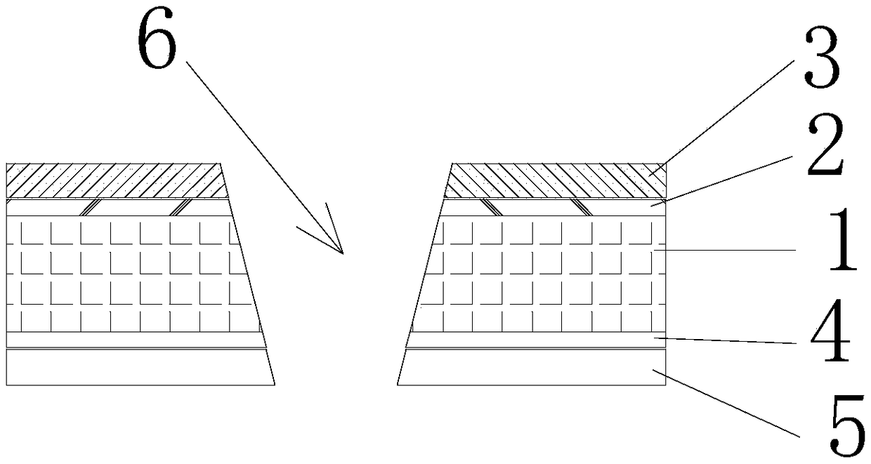
[0023] Follow the steps below to fabricate a COF flexible substrate that avoids voids in vias:

[0024] (1) Laser drilling: on the upper surface of the polyimide intermediate layer 1, an upper metal Ni / Cr layer 2 with a thickness of 20nm is set, and at the lower surface of the polyimide intermediate layer 1, a lower metal Ni with a thickness of 20nm is set. / Cr layer 4, an upper copper layer 3 with a thickness of 1 μm is set on the upper surface of the upper metal Ni / Cr layer 2, and a lower copper layer 5 with a thickness of 1 μm is set on the lower surface of the lower metal Ni / Cr layer 4 to make a base material, On the base material, a through hole 6 that runs through the entire base material is lasered. The laser adopts an impact method, and the number of impacts is 12 times. The upper aperture of the through hole 6 is 25 μm, and the lower aperture of the through hole 6 is 15 μm;

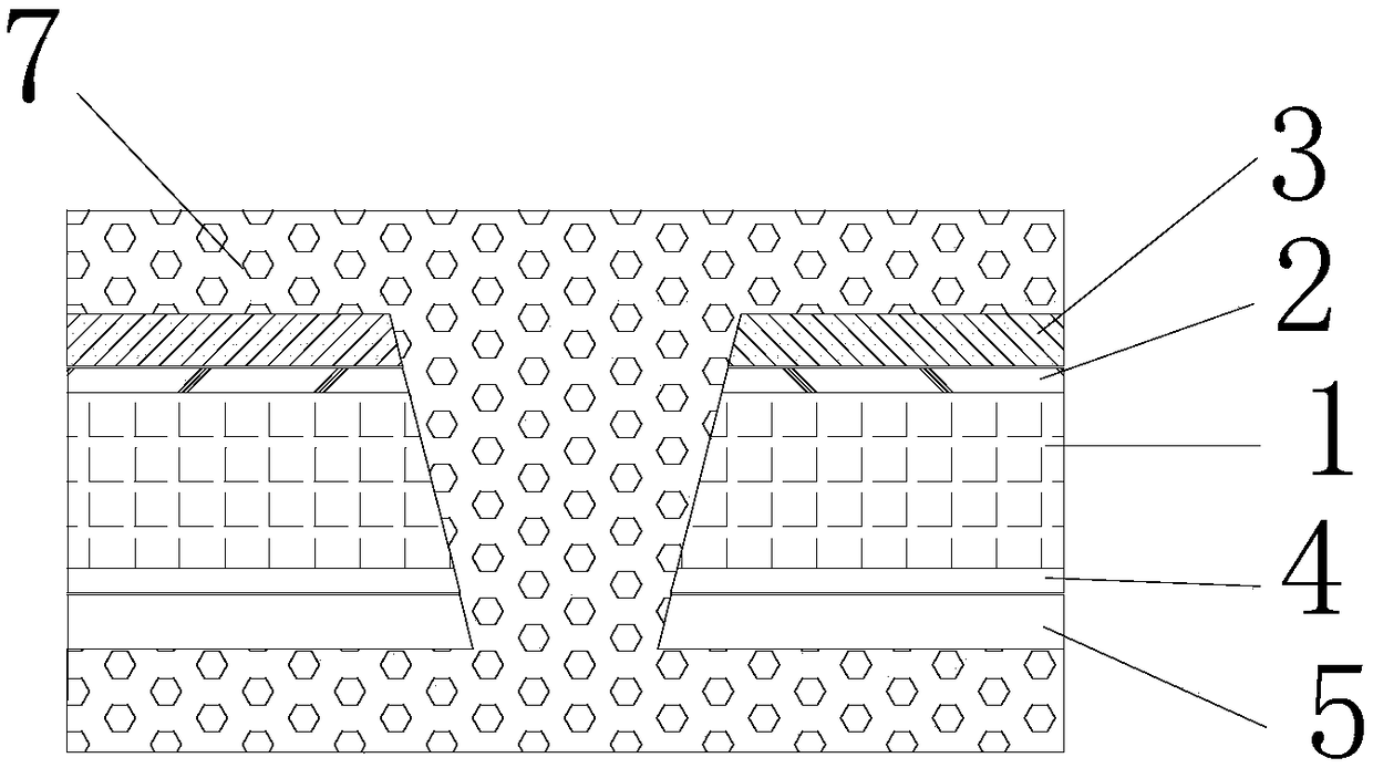
[0025] (2) In-hole coating: deposit a conductive carbon film on the inner wall of the through...

Embodiment 2

[0028] The difference from Example 1 is that in step (1), the number of impacts is 10, and the lower diameter of the through hole 6 is 11 μm.

Embodiment 3

[0030] The difference from Example 1 is that in step (1), the number of impacts is 11, and the lower hole diameter of the through hole 6 is 14 μm.


PUM


Abstract

The invention provides a manufacturing method for a COF flexible substrate and capable of avoiding cavities in through holes, comprising the following steps: (1) performing laser drilling; (2) coatingfilms in the through holes; and (3) filling the through holes and electroplating copper. The invention also provides a product obtained by adopting the manufacturing method. The manufacturing methodprovided by the invention can form the through holes with different up-down apertures by virtue of lasers, thus the cavities in the through holes are effectively avoided.

Description

technical field [0001] The invention relates to a method for manufacturing a COF flexible substrate capable of avoiding cavities in through holes and its products. Background technique [0002] COF (Chip on film, chip on film technology), is to mount the chip on a flexible film substrate to realize the output of the chip I / O, and is widely used in the panels of mobile phones, TVs, ipads and other electronic products. At present, enterprises that master the production technology of COF flexible substrates and have the conditions for large-scale mass production are concentrated in South Korea, Japan, and Taiwan, China; some domestic enterprises have the production capacity of producing COF flexible substrates. With the rise of OLED in the panel industry, the demand for COF flexible substrates demand will increase. Domestic enterprises urgently need to improve the technical capabilities of COF flexible substrates. In addition to the line width / line spacing of COF flexible sub...

Claims


Application Information

Patent Timeline
Patent Type & Authority Applications(China)
IPC IPC(8): H05K3/00H05K3/42
CPCH05K3/0047H05K3/422
Inventor 张俊杰万克宝刘清
Owner MFLEX YANCHENG CO LTD
Why Eureka
Try Eureka