Complementary metal oxide semiconductor (CMOS)-based high-response working method for terahertz sensor
A working method, terahertz technology, applied to radiation control devices, etc., can solve the problems of increased production cost and manufacturing difficulty, achieve low noise equivalent power, reduce noise equivalent power, and increase voltage response
- Summary
- Abstract
- Description
- Claims
- Application Information
AI Technical Summary
Problems solved by technology
Method used
Image
Examples
Embodiment Construction
[0030] The proposed scheme will be described in detail below in conjunction with the accompanying drawings.
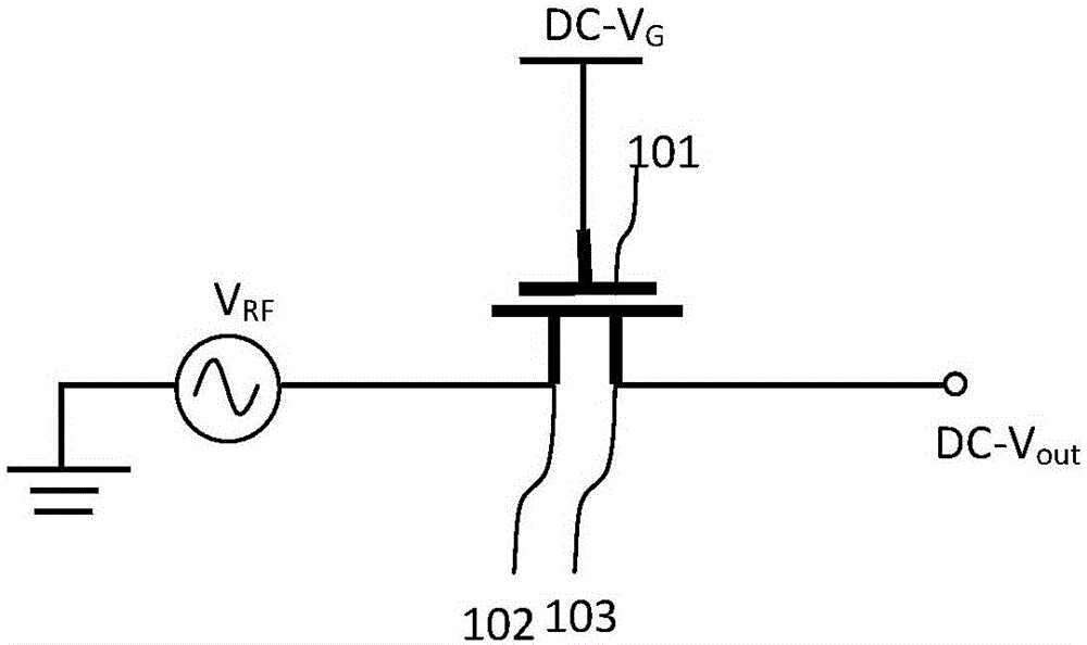
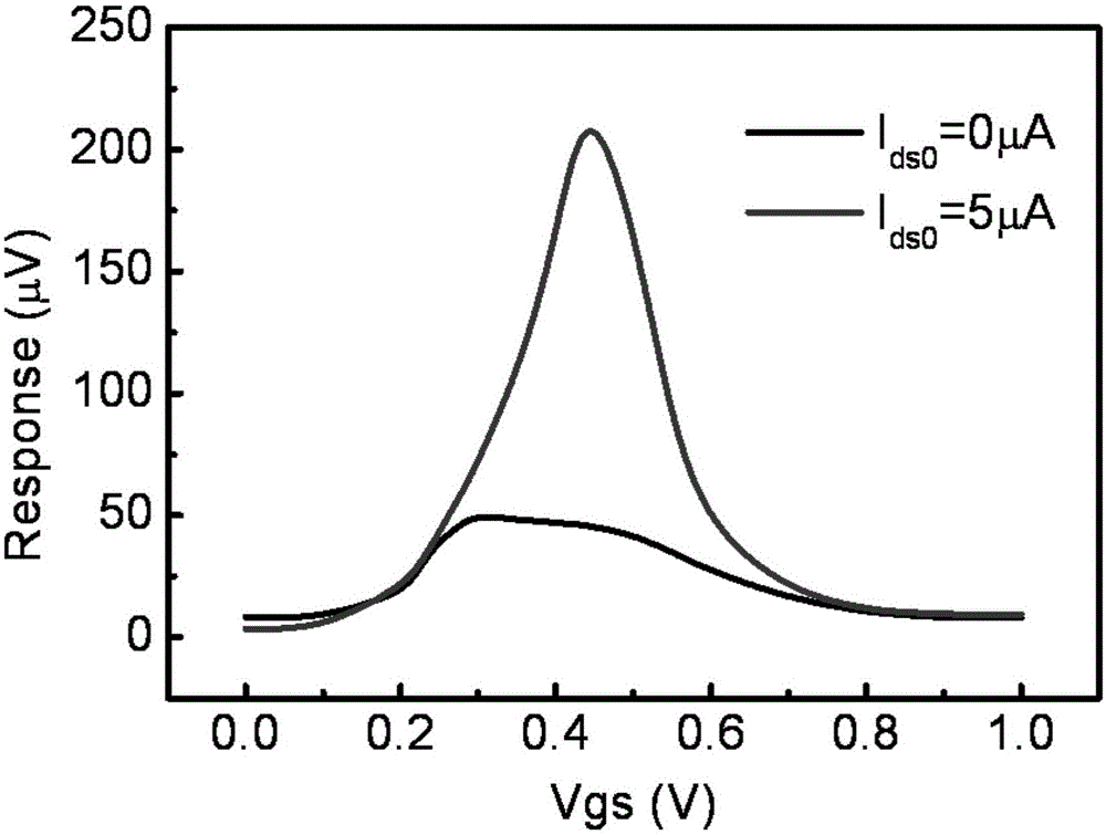
[0031] In this example, a standard 0.18μm semiconductor process is used to manufacture a terahertz sensor, in which the transistor size is 0.18μm×1μm, and a 650GHz antenna is integrated to collect terahertz signals. We first let this terahertz sensor work in conventional mode. Such as figure 1 As shown, a DC bias voltage V is applied to the gate (101) gs, the terahertz signal collected by the antenna is input from the source terminal (102), the drain terminal (103) is floating, and is connected with a lock-in amplifier to output a voltage. image 3 The middle black curve represents the voltage response and DC bias V of the terahertz sensor in this example in the traditional working mode gs It can be seen that the maximum response voltage at this time is about 50μV.
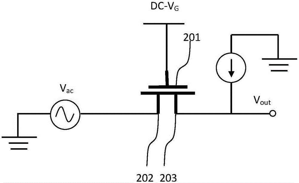
[0032] Then we let the same terahertz sensor work in the novel working mode proposed by the present...
PUM
 Abstract
Description
Claims
Application Information


