A terahertz detector based on a non-self-aligned cmos structure

A terahertz detector and area technology, applied in the field of MOSFET and terahertz detector, can solve the problem of MOSFET terahertz detection performance degradation, etc., to improve the output voltage response RV, reduce the overlap capacitance, reduce the noise equivalent The effect of power

Active Publication Date: 2018-03-13
NANJING UNIV
View PDF3 Cites 0 Cited by
  • Summary
  • Abstract
  • Description
  • Claims
  • Application Information

AI Technical Summary

Problems solved by technology

The larger the size of the overlap area, the larger the source-gate overlap capacitance, resulting in lower performance of MOSFET-based terahertz detection.

Method used


Image

  • A terahertz detector based on a non-self-aligned cmos structure
  • A terahertz detector based on a non-self-aligned cmos structure
  • A terahertz detector based on a non-self-aligned cmos structure

Examples


Embodiment Construction

[0027] In order to make the content of the present invention clearer, the implementation manner of the present invention will be further described in detail below in conjunction with the accompanying drawings.

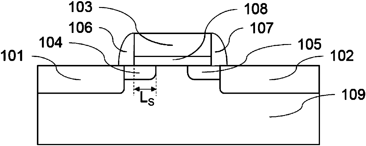
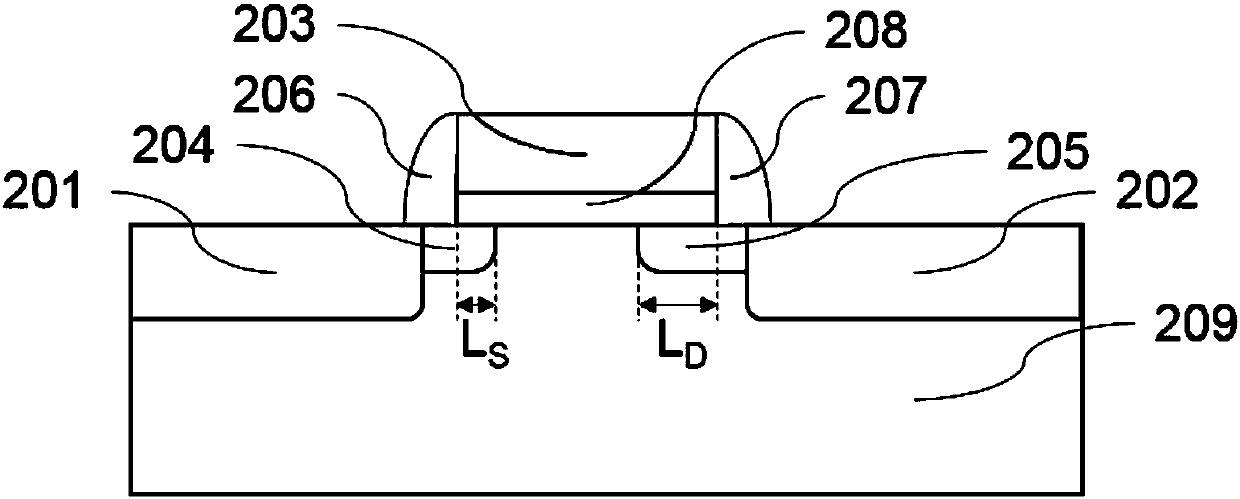
[0028] figure 2 It is a cross-sectional structure diagram of a MOSFET that can effectively improve the performance of a terahertz detector described in the present invention. The MOSFET device is fabricated on a p-type substrate 209, the two n-type doped regions are the source region 201 and the drain region 202, the heavily doped polysilicon region is the gate 203, and the gate and the substrate are SiO 2 layer 208, the MOSFET source region 201 and drain region 202 are distributed asymmetrically with respect to the polysilicon gate 203; figure 1 The length of the LDD 104 diffused to the gate region 103 in the traditional MOSFET source region produced by the self-aligned CMOS process technology shown; the overlapping area of ​​the source region 201 and the gate regio...


PUM


Abstract

The invention relates to a Terahertz detector of a MOSFET structure based on a non-self-aligning CMOS structure. Two n-type doped areas on a p-type substrate 209 are a source area and a drain area respectively, a SiO2 layer is placed on the centers of the source area and the drain area, a heavily-doped polysilicon area serves as the grid, the SiO2 layer is placed between the grid and a substrate, the source-end area and the drain-end area of the MOSFET are distributed in an asymmetric manner relative to the polysilicon grid, the length that LDD of the source-end area is diffused to position under the grid area is lower than the length that LDD of the drain-end area is diffused to position under the grid area, or the lens that LDD of the source-end area is diffused to position under the grid area is lower than the length LDD 104 of the source-end area of a traditional MOSFET using the self-aligning technology to position under the grid area, the overlapped area between the source-end area and the grid area of the MOSFET is lower than the source-grid overlapped area of the traditional MOSFET, and the side surface of the grid includes sidewall silicon oxide.

Description

technical field [0001] The invention relates to the fields of terahertz detectors and MOSFETs, in particular to a MOSFET structure using a non-self-aligned CMOS process, which can effectively improve the performance of terahertz detectors. Background technique [0002] Terahertz is an electromagnetic wave with a frequency between infrared and microwave. Due to the high spatial and temporal resolution of terahertz, terahertz imaging technology has become one of the current research hotspots. At the same time, many non-metallic polar materials have little absorption of terahertz rays, so they can detect the internal information of the material. In addition, the terahertz electromagnetic energy is small and will not damage the material, and the resonance frequency of the vibration and rotation frequency of biomolecules is in the Therefore, terahertz has broad application prospects in the fields of security inspection and medical imaging. [0003] Terahertz detector is one of ...

Claims


Application Information

Patent Timeline
Patent Type & Authority Patents(China)
IPC IPC(8): H01L29/78H01L29/08H01L29/66H01L21/266
CPCH01L21/266H01L29/0847H01L29/66568H01L29/7833
Inventor 纪小丽张行行闫锋朱颖杰廖轶明
Owner NANJING UNIV
Why Eureka
Try Eureka