Low temperature poly silicon thin film transistor and fabrication method thereof

A thin-film transistor and low-temperature polysilicon technology, applied in transistors, semiconductor/solid-state device manufacturing, semiconductor devices, etc., can solve problems such as large leakage current of displays, and achieve the effect of reducing sub-threshold swing and leakage current.

Inactive Publication Date: 2015-12-09
WUHAN CHINA STAR OPTOELECTRONICS TECH CO LTD
View PDF4 Cites 9 Cited by
  • Summary
  • Abstract
  • Description
  • Claims
  • Application Information

AI Technical Summary

Problems solved by technology

[0005] In view of this, the present invention provides a low-temperature polysilicon thin-film transistor and its manufacturing method to solve the problem that low-temperature polysilicon thin-film transistor displays in the prior art tend to generate relatively large leakage currents

Method used


Image

  • Low temperature poly silicon thin film transistor and fabrication method thereof
  • Low temperature poly silicon thin film transistor and fabrication method thereof
  • Low temperature poly silicon thin film transistor and fabrication method thereof

Examples


Embodiment Construction

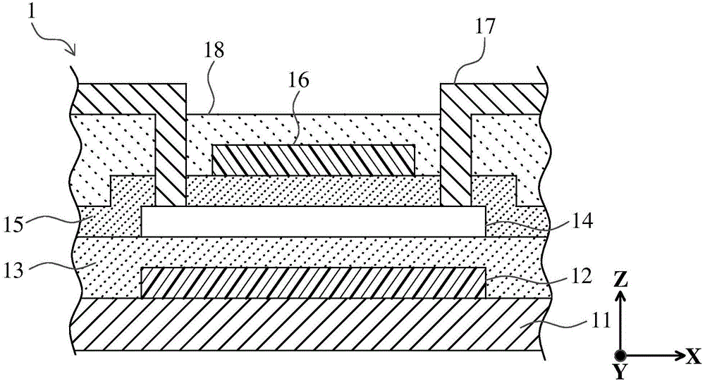
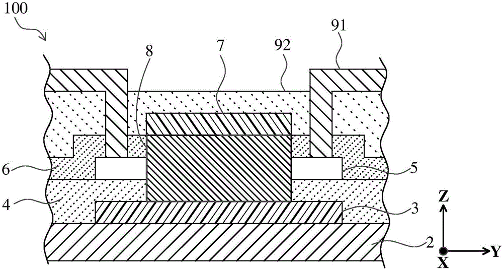
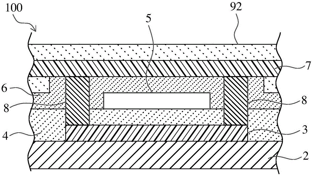
[0025] The following descriptions of the various embodiments refer to the accompanying drawings to illustrate specific embodiments in which the present invention can be practiced. Furthermore, the directional terms mentioned in the present invention are, for example, up, down, top, bottom, front, back, left, right, inside, outside, side, surrounding, central, horizontal, transverse, vertical, longitudinal, axial, The radial direction, the uppermost layer or the lowermost layer, etc. are only directions referring to the attached drawings. Therefore, the directional terms used are used to illustrate and understand the present invention, but not to limit the present invention.

[0026] Please refer to figure 2 , 3 Shown is a preferred embodiment of the low temperature polysilicon (LowtemperaturePolysilicon; LTPS) thin film transistor of the present invention, wherein figure 2 is along the X-axis direction (horizontal and horizontal, such as figure 2 The schematic diagram o...


PUM


Abstract

The invention discloses a low temperature poly silicon thin film transistor and a fabrication method thereof. The low temperature poly silicon thin film comprises a substrate, a shading layer, a buffer layer, a poly silicon layer, a gate insulation layer, a gate and at least gate surrounding channel. With the design of the gate surrounding channel, the leakage current generated by the thin film transistor can be effectively reduced.

Description

technical field [0001] The present invention relates to a thin film transistor and its manufacturing method, in particular to a low temperature polysilicon thin film transistor and its manufacturing method. Background technique [0002] Thinfilm transistor liquid crystal display (TFT-LCD) is divided into polysilicon technology and non-polysilicon technology. Low temperature polysilicon (LTPS) technology is a new generation of thin film transistor display manufacturing technology. The biggest difference from traditional non-polysilicon displays lies in the response speed of low temperature polysilicon displays. Faster, and has the advantages of high brightness, high resolution and low power consumption. [0003] Such as figure 1 As shown, it is a schematic diagram of a cross section of an existing low-temperature polysilicon thin film transistor display 1 along an X-axis direction (horizontal transverse direction), and the low temperature polysilicon thin film transistor dis...

Claims


Application Information

Patent Timeline
Patent Type & Authority Applications(China)
IPC IPC(8): H01L29/786H01L21/336
CPCH01L29/78675H01L29/66757
Inventor 陈归赵莽
Owner WUHAN CHINA STAR OPTOELECTRONICS TECH CO LTD
Why Eureka
Try Eureka