Fabrication method for printed circuit board (PCB) with irregularity in board surface

A technology of PCB board and manufacturing method, which is applied in the field of manufacturing uneven PCB boards to achieve the effect of improving the production yield

Active Publication Date: 2015-12-09
SHENZHEN KINWONG ELECTRONICS
View PDF3 Cites 11 Cited by
  • Summary
  • Abstract
  • Description
  • Claims
  • Application Information

AI Technical Summary

Problems solved by technology

[0006] In view of the above-mentioned deficiencies in the prior art, the object of the present invention is to provide a method fo

Method used


Image

  • Fabrication method for printed circuit board (PCB) with irregularity in board surface
  • Fabrication method for printed circuit board (PCB) with irregularity in board surface
  • Fabrication method for printed circuit board (PCB) with irregularity in board surface

Examples


Embodiment Construction

[0024] The present invention provides a method for manufacturing a PCB with an uneven board surface. In order to make the purpose, technical solution and effect of the present invention clearer and clearer, the present invention will be further described in detail below. It should be understood that the specific embodiments described here are only used to explain the present invention, not to limit the present invention.

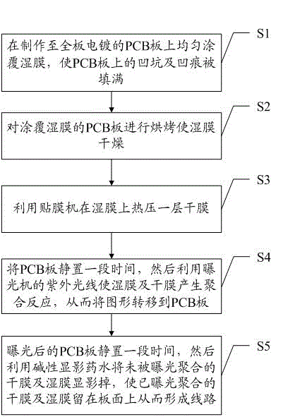
[0025] see figure 1 , figure 1 It is a flow chart of a preferred embodiment of a method for manufacturing an uneven PCB board of the present invention, wherein it includes steps:

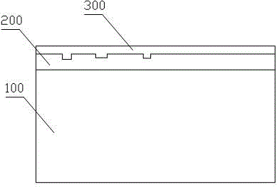
[0026] S1. Evenly coat the wet film on the PCB plated to the full plate, so that the pits and dents on the PCB are filled;

[0027] S2, baking the PCB board coated with the wet film to dry the wet film;

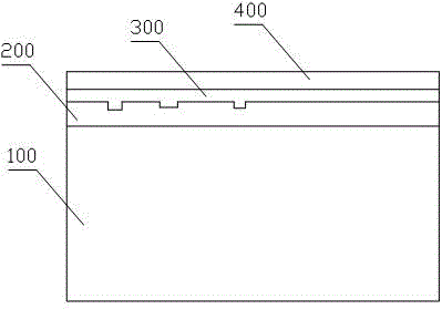
[0028] S3, hot pressing a layer of dry film on the wet film by using a film laminating machine;

[0029] S4. Let the PCB board stand for a period of time, and then use the ul...


PUM


Abstract

The invention discloses a fabrication method for a printed circuit board (PCB) with irregularity in a board surface. The fabrication method comprises the following steps of: A, uniformly applying a wet film onto the PCB with plating on the whole board to make pits and dents on the PCB filled; B, roasting the PCB coated with the wet film to dry the wet film; C, hot-pressing a layer of dry film on the wet film by using a film lamination machine; D, allowingthe PCB to stand for a certain time, and leading the wet film and the dry film to have a polymerization reaction by using ultraviolet light rays of an exposure machine so as to transfer a pattern to the PCB; and E, allowing the PCB to stand for a certain time after an exposure, developing the dry film and the wet film which are not exposed and polymerized by using an alkaliphotograph potion, and leading the dry film and the wet film which are exposed and polymerized already to be reserved on the board surface so as to form a circuit. By the fabrication method, the problems of a gap and an open circuit appearing after etching the PCB with irregularity in the board surface are solved, and the fabrication yield is enhanced.

Description

technical field [0001] The invention relates to the field of PCB manufacturing, in particular to a method for manufacturing a PCB with an uneven board surface. Background technique [0002] The dry film is a photosensitive resist layer. After being irradiated by ultraviolet light, the photosensitive part undergoes a polymerization reaction and adheres stably to the PCB surface. The non-photosensitive part is washed away by liquid medicine to form a resist layer that blocks electroplating and etching. [0003] The normal PCB board surface should be flat, but some board surfaces may have pits and dents on the board surface due to handling, operation, pressing, and even electroplating during the previous process. When the dry film of the resist layer is attached to the PCB with serious pits and dents, it will not be tightly attached, and the film will be thrown off after development, and then the lines, holes, PAD and copper surface will be notched after etching at the pits and...

Claims


Application Information

Patent Timeline
IPC IPC(8): H05K3/00
CPCH05K3/0085H05K2203/0759
Inventor 张霞王俊曾平
Owner SHENZHEN KINWONG ELECTRONICS
Why Eureka
Try Eureka