High-power device fan-out packaging structure and production process

A technology of packaging structure and production process, applied in the direction of electric solid state device, semiconductor device, semiconductor/solid state device manufacturing, etc., can solve the problems of thermal management performance limitation, complex process, low performance, etc., to solve the dependence of patch process equipment , the process is simple, the effect of low cost

Active Publication Date: 2018-04-17
NAT CENT FOR ADVANCED PACKAGING CO LTD
View PDF4 Cites 0 Cited by
  • Summary
  • Abstract
  • Description
  • Claims
  • Application Information

AI Technical Summary

Problems solved by technology

[0003] At present, the mainstream fan-out packaging is still based on the injection molding (molding) method based on the wafer process. The main fan-out RDL uses sputtered metal film as the seed layer or wafer. The heat dissipation of the package made by this structure The management performance is very limited; in addition, the process is also characterized by high cost and complicated process, which leads to high cost and low performance.

Method used


Image

  • High-power device fan-out packaging structure and production process
  • High-power device fan-out packaging structure and production process
  • High-power device fan-out packaging structure and production process

Examples


Embodiment Construction

[0048] The present invention will be further described below in conjunction with specific drawings.

[0049] The present disclosure will be described more fully hereinafter with reference to the accompanying drawings, in which embodiments of the disclosure are shown. These embodiments may, however, be embodied in many different forms and should not be construed as limited to the embodiments set forth herein. Rather, these examples are provided so that this disclosure will be thorough and complete, and will fully convey the scope of the disclosure to those skilled in the art. It should be noted that although a relatively complete manufacturing process of a chip package device will be described below, some process steps are optional and there are alternative implementations.

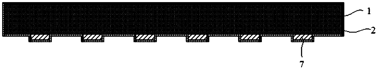
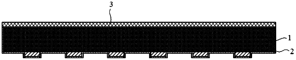
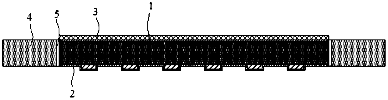
[0050] Such as Figure 15 As shown, the high-power device fan-out packaging structure includes a core board 4, and a slot body 5 connecting the front and back sides of the core board 4 is opened on the c...


PUM


Abstract

The invention relates to a high-power device fan-out packaging structure and production process, which is characterized in that it includes a core board, and a chip is arranged in a groove on the core board; the core board, the chip, the lower dielectric material and the upper dielectric material are pressed together together; the upper dielectric material is located directly above the back of the core board, a metal layer is provided on the surface of the upper dielectric material, an opening is provided on the upper dielectric material, the opening is located directly above the back of the chip, and a heat sink is filled in the opening; A solder resist layer is provided on the lower surface of the lower dielectric material, an RDL circuit layer is arranged in the solder resist layer, BGA balls are arranged on the pads of the RDL circuit layer; laser blind holes are provided on the lower dielectric material, The electroplated metal is filled in the laser blind hole, and the RDL circuit layer is interconnected with the pad on the front side of the chip through the electroplated metal in the laser blind hole. A resin layer is coated on the surface of the chip. The invention solves the heat dissipation problem of fan-out packaging of high-power devices; and the process is simple and compatible with most chips.

Description

technical field [0001] The invention relates to a high-power device fan-out packaging structure and production technology, belonging to the field of microelectronic advanced packaging technology. Background technique [0002] The traditional fan-out packaging structural components are embedded in resin and dissipate heat through the front side. This structure has relatively large thermal resistance and is suitable for packaging low-power devices. [0003] At present, the mainstream fan-out packaging is still based on the injection molding (molding) method based on the wafer process. The main fan-out RDL uses sputtered metal film as the seed layer or wafer. The heat dissipation of the package made by this structure The management performance is very limited; in addition, the process is also characterized by high cost and complicated process, which leads to high cost and low performance. Contents of the invention [0004] The purpose of the present invention is to overcome ...

Claims


Application Information

Patent Timeline
Patent Type & Authority Patents(China)
IPC IPC(8): H01L23/31H01L23/367H01L21/56H01L21/60
CPCH01L2224/04105H01L2224/12105H01L2224/19H01L2224/32245H01L2224/73267H01L2224/92244
Inventor 郭学平郝虎
Owner NAT CENT FOR ADVANCED PACKAGING CO LTD
Why Eureka
Try Eureka