Visible light communication led devices
A technology for LED devices and visible light communication, applied in the field of visible light communication, can solve the problem that the system performance needs to be further improved, and achieve the effect of improving the response time and improving the composite rate.
- Summary
- Abstract
- Description
- Claims
- Application Information
AI Technical Summary
Problems solved by technology
Method used
Image
Examples
Embodiment Construction
[0018] The implementation of the present invention will be further described below in conjunction with the accompanying drawings and examples, but the implementation and protection of the present invention are not limited thereto.
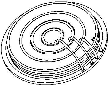
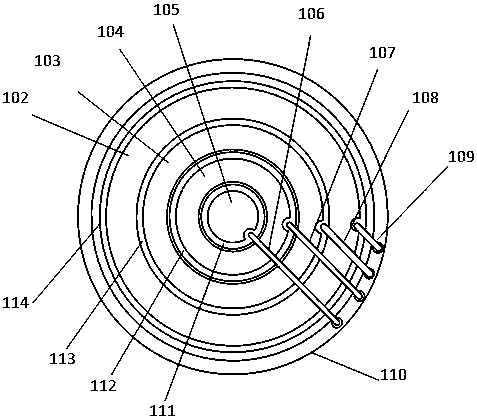
[0019] according to figure 1 , figure 2 and image 3 Structure, choose GaN material, use metal organic chemical vapor phase deposition (MOCVD) technology, grow GaN / InGaN material epitaxial wafer, use semiconductor plane process line, prepare four chips (the middle chip is circular), in each chip On the other hand, the ring-shaped metal positive electrode is prepared by evaporation or sputtering, and the material can be Al or graphene. Such as figure 1 , the visible light communication LED device includes four LED chips whose geometric center points overlap and are located on the same plane. The edge of the chip is wound with a ring-shaped metal positive electrode, wherein a first metal ring-shaped positive electrode 111 is provided on the midd...
PUM
 Abstract
Description
Claims
Application Information


