A fabrication method for Gan-based LED chips capable of high-efficiency encapsulation

An LED chip, high-efficiency technology, used in semiconductor/solid-state device manufacturing, electrical components, electrical solid-state devices, etc., can solve the problems of low production efficiency, high defect rate, poor reliability, etc., to achieve low cost, stable and reliable product performance. good effect

Active Publication Date: 2017-11-24
SHANDONG INSPUR HUAGUANG OPTOELECTRONICS
View PDF3 Cites 0 Cited by
  • Summary
  • Abstract
  • Description
  • Claims
  • Application Information

AI Technical Summary

Problems solved by technology

[0006] Aiming at the disadvantages of low production efficiency, high defect rate, and poor reliability in the packaging production and processing process of the existing single LED chip, the present invention provides a LED chip with high optical power, high packaging efficiency, high yield, and good reliability. Preparation method of GaN-based LED chip with low packaging cost and high-efficiency packaging

Method used


Image

  • A fabrication method for Gan-based LED chips capable of high-efficiency encapsulation
  • A fabrication method for Gan-based LED chips capable of high-efficiency encapsulation
  • A fabrication method for Gan-based LED chips capable of high-efficiency encapsulation

Examples


Embodiment Construction

[0025] The method for preparing a GaN-based LED chip that can realize high-efficiency packaging of the present invention includes the following steps:

[0026] (1) Preparation of epitaxial wafers

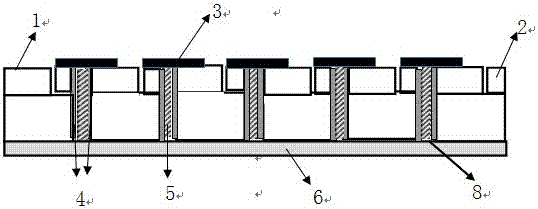
[0027] Such as figure 1 As shown, an epitaxial layer is grown on the substrate 6 to form an epitaxial wafer; the epitaxial layer is sequentially composed of a GaN layer, an N-type GaN layer, a quantum well active region, and a P-type GaN layer from bottom to top; in order to effectively activate the P For the activity of doping impurities in the GaN layer, a transparent conductive layer of ITO with a thickness of 2000-2500 angstroms is evaporated on the surface of the epitaxial wafer by using a metal evaporation platform.

[0028] (2) Making P electrodes and N electrodes

[0029] Use photoresist as a mask to make P electrode patterns and N electrode patterns on the surface of the epitaxial wafer; remove the photoresist mask outside the electrode pattern by wet etching, anneal the ...


PUM


Abstract

A method for preparing a GaN-based LED chip capable of achieving high-efficiency packaging, comprising the following steps: (1) preparing an epitaxial wafer, and evaporating a layer of ITO transparent conductive layer on the surface of the epitaxial wafer; (2) making a P electrode and an N electrode; The photoresist mask on the electrode and the N electrode will not be removed temporarily; (3) cutting the epitaxial wafer to form a single chip unit, cutting to the substrate, so that isolation grooves are formed between adjacent chip units; (4) ) Deposit SiO2 on the surface of the epitaxial wafer with isolation grooves, and use wet etching to remove the photoresist mask on the surface of the chip electrode; (5) carry out metallization connection to the chip unit; (6) cut out the required parts according to the packaging requirements LED chips. The invention pre-connects the LED chips in series and parallel, and then performs the packaging process; the corresponding chips can be cut out according to the requirements, and can be packaged directly, which has the advantages of convenient operation of the packaging process, high packaging efficiency, low cost, stable product performance, High luminous efficiency, good reliability and so on.

Description

technical field [0001] The invention relates to a method for preparing a GaN-based LED chip, belonging to the technical field of LED chip preparation. Background technique [0002] As the core component of semiconductor lighting, LED chips are faced with increasingly severe market conditions, and higher requirements are put forward for the manufacturing methods of LED chips in terms of how to increase the optical power of chips, improve packaging efficiency, and reduce packaging costs. As we all know, after the production and processing of LED chips is completed, the chips need to be packaged into LED lamp beads. The chip presented in the current LED market is to divide the complete epitaxial wafer into individual small units after the tube core process is completed. Each unit is an LED chip, and each chip has a positive pole, a Negative electrode, when packaging, each LED chip unit needs to be fixed on an LED bracket, and then use special wire bonding equipment to connect ...

Claims


Application Information

Patent Timeline
Patent Type & Authority Patents(China)
IPC IPC(8): H01L33/52H01L25/075H01L21/56H01L21/60
CPCH01L21/561H01L24/91H01L33/52H01L2224/9205
Inventor 曹志芳夏伟闫宝华徐现刚
Owner SHANDONG INSPUR HUAGUANG OPTOELECTRONICS
Why Eureka
Try Eureka