Complementary metal oxide semiconductor image sensor and manufacturing method thereof

An oxide semiconductor and image sensor technology, which is applied in semiconductor/solid-state device manufacturing, radiation control devices, electrical components, etc., can solve the problems of unstoppable lateral diffusion of photogenerated carriers, large absorption depth of long-wavelength light, imaging resolution and Problems such as the adverse effects of color noise can be achieved to improve the quantum efficiency of photoelectric conversion and improve the ability of double anti-signal crosstalk

Active Publication Date: 2017-08-25
QIXINRUIHUA TECH WUHAN CO LTD
View PDF4 Cites 0 Cited by
  • Summary
  • Abstract
  • Description
  • Claims
  • Application Information

AI Technical Summary

Problems solved by technology

However, the depletion depth of silicon substrates in this way is still limited
Moreover, because of the large absorption depth of long-wavelength light, the carriers generated deep in the substrate easily exceed the control area of ​​the drift electric field and diffuse laterally into adjacent pixels, resulting in signal crosstalk.
In addition, if the isolation barrier between adjacent pixels is not deep enough for the deep region of the substrate, it will not be able to prevent the lateral diffusion of photogenerated carriers, and signal crosstalk will easily occur.
The signal crosstalk caused by this lateral diffusion will adversely affect the imaging resolution and color noise in low light

Method used


Image

  • Complementary metal oxide semiconductor image sensor and manufacturing method thereof
  • Complementary metal oxide semiconductor image sensor and manufacturing method thereof

Examples


Embodiment Construction

[0025] Below in conjunction with accompanying drawing and embodiment the present invention is described in further detail:

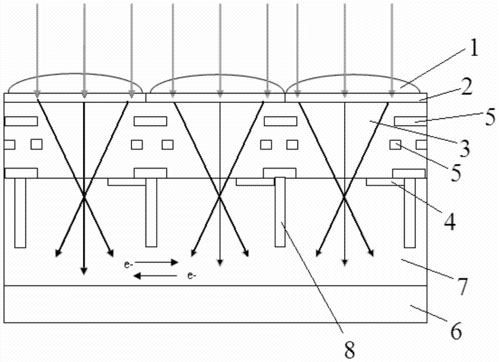
[0026] The CMOS image sensor of the present invention, such as figure 2 As shown, it includes an optical filter 2, a photosensitive working circuit unit 4, a silicon substrate 6, a microlens array 1 (formed by a plurality of microlenses arranged side by side) arranged on the top surface of the optical filter 2, and an array of microlenses arranged on the optical filter 2. 2 the metal interconnection medium layer 3 on the bottom surface, the metal interconnection layer 5 matched with the photosensitive working circuit unit 4 and located in the metal interconnection medium layer 3, the silicon substrate epitaxial layer 7 located on the top surface of the silicon substrate 6, and the photosensitive working circuit unit 4 Set in the epitaxial layer 7 of the silicon substrate, the photosensitive working circuit unit 4 is used to control the pixel unit operat...


PUM


Abstract

The invention discloses a complementary metal oxide semiconductor image sensor, which comprises a light filter, a photosensitive working circuit unit, a silicon substrate, a microlens array, a metal interconnection medium layer, a metal interconnection layer, a silicon substrate epitaxial layer, and a microlens The silicon substrate epitaxial layer corresponding to the silicon substrate epitaxial layer under each microlens of the array and the photosensitive working circuit unit in the corresponding silicon substrate epitaxial layer area are a pixel unit, and also include a silicon substrate reflective curved surface block array arranged on the bottom surface of the silicon substrate, The curved surface layer of the reflective curved surface block array of the silicon substrate is provided with a reflective medium layer, and a pixel isolation barrier is provided between two adjacent pixel units, and each pixel isolation barrier extends downward to pass through the silicon substrate. The invention can improve the photoelectric conversion quantum efficiency, reduce carrier signal crosstalk, and improve the imaging quality of an image sensor in a dark field environment.

Description

technical field [0001] The invention belongs to the technical field of semiconductor solid-state imaging devices, and in particular relates to a complementary metal oxide semiconductor image sensor and a manufacturing method thereof. [0002] technical background [0003] Complementary metal oxide image sensors are easy to integrate on-chip systems because their manufacturing processes are compatible with signal processing chips and other manufacturing processes. Noise ratio, so it has an advantage in the field of image sensor applications. [0004] An important feature index of an image sensor is light sensitivity, especially in low-light application environments, which plays a key role in image quality. Existing image sensors such as figure 1 As shown, it includes an optical filter 2, a photosensitive working circuit unit 4, a silicon substrate 6, a microlens array 1 arranged on the top surface of the optical filter 2, a metal interconnection medium layer 3 arranged on th...

Claims


Application Information

Patent Timeline
Patent Type & Authority Patents(China)
IPC IPC(8): H01L27/146H01L21/8238
Inventor 李潇
Owner QIXINRUIHUA TECH WUHAN CO LTD
Why Eureka
Try Eureka