Array substrate, manufacturing method, and display device

An array substrate and array technology, which is applied in semiconductor/solid-state device manufacturing, organic semiconductor devices, electrical components, etc., can solve the problems that array substrates cannot meet performance requirements, and cannot realize the integration of scanning drive circuits and data drive circuits, etc., to achieve increased Effects of screen display area, size reduction, and display resolution improvement

Inactive Publication Date: 2015-12-23
BOE TECH GRP CO LTD +1
View PDF7 Cites 17 Cited by
  • Summary
  • Abstract
  • Description
  • Claims
  • Application Information

AI Technical Summary

Problems solved by technology

Based on the above reasons, the array substrate formed by the existing process cannot meet the performance requirements of other circuit modules integ...

Method used


Image

  • Array substrate, manufacturing method, and display device
  • Array substrate, manufacturing method, and display device
  • Array substrate, manufacturing method, and display device

Examples


Embodiment Construction

[0054] In order to make the purpose, technical solutions and advantages of the embodiments of the present invention clearer, the technical solutions in the embodiments of the present invention will be clearly and completely described below in conjunction with the drawings in the embodiments of the present invention. Obviously, the described embodiments It is a part of embodiments of the present invention, but not all embodiments. Based on the embodiments of the present invention, all other embodiments obtained by persons of ordinary skill in the art without creative efforts fall within the protection scope of the present invention.

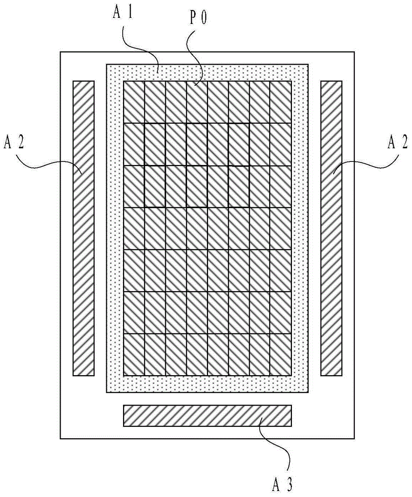
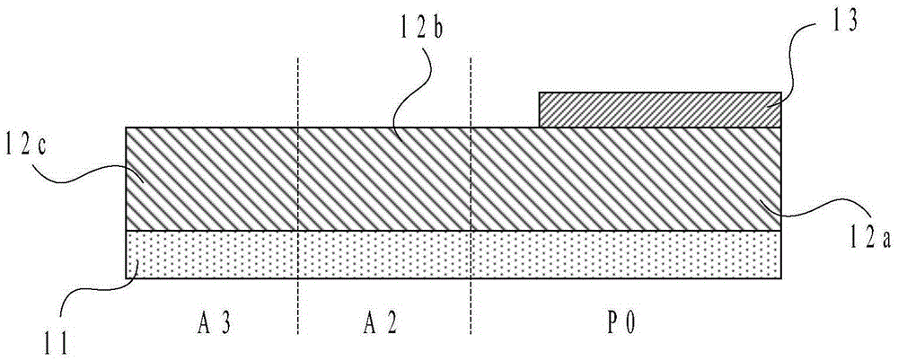
[0055] Figure 1A and Figure 1B It is a schematic structural diagram of an array substrate in an embodiment of the present invention. see Figure 1A and Figure 1B , the array substrate includes a single crystal silicon substrate 11 , an array circuit layer 12 and an anode conductive layer 13 . Wherein, the single crystal silicon substrate 11 ...


PUM


Abstract

The invention provides an array substrate, a manufacturing method, and a display device. The array substrate comprises a monocrystalline silicon substrate, an array circuit layer, and an anode conducting layer. The monocrystalline silicon substrate is provided with a central display region, a first peripheral region, and a second peripheral region. The central display region comprises a plurality of pixel regions. The array circuit layer is formed on the monocrystalline silicon substrate, and comprises a plurality of transistors which are formed in the monocrystalline silicon substrate in an active region. The array circuit layer forms a scanning drive circuit in the first peripheral region, forms a data drive circuit in the second peripheral region, and forms a pixel circuit in each pixel region. The anode conducting layer is formed on an array circuit layer in each pixel region, and is used for outputting an organic light-emitting layer drive current in each pixel region and reflecting light from an organic light-emitting layer. According to the invention, the integrated manufacturing of the scanning drive circuit and the data drive circuit on the substrate is achieved, and the improvement of display performance is facilitated.

Description

technical field [0001] The present invention relates to the field of display technology, in particular to an array substrate, a manufacturing method thereof, and a display device. Background technique [0002] Gated driver On Array (GOA) technology, as a new display technology, integrates the scanning driving circuit on the array substrate to remove the part of the scanning driving integrated circuit, thereby saving materials and reducing process steps, and achieving the goal of reducing product cost. Purpose. However, in addition to the scanning driving circuit, other circuits are rarely integrated and fabricated on the array substrate in the prior art. The main reason is that, for example, the circuit module of the data driving circuit is more complicated than the structure of the scanning driving circuit. If it is to be fabricated on a glass substrate, it needs to occupy a considerable area, so it is bound to compress the area of ​​the display area. area. In addition, ...

Claims


Application Information

Patent Timeline
IPC IPC(8): H01L27/32H01L21/77
CPCH01L21/8234H01L21/84H01L29/78654H01L27/12H10K59/1213H10K2102/3026H10K59/124H10K59/131H10K50/81H10K50/818H10K50/828H10K59/122H10K59/123H10K71/00H01L21/02164H01L21/0217H01L21/26513H01L21/266H01L21/76802H01L21/76877H01L27/1222H01L27/124H01L27/1248H01L27/1262H01L29/66772
Inventor 赖韦霖詹裕程黄建邦
Owner BOE TECH GRP CO LTD
Why Eureka
Try Eureka