pbn type ingaas infrared detector

An infrared detector, n-type technology, applied in the direction of semiconductor devices, electrical components, circuits, etc., to achieve the effects of suppressing the generation of dark current, reducing requirements and device costs, and reducing surface recombination

Inactive Publication Date: 2017-01-25
CHANGCHUN INST OF OPTICS FINE MECHANICS & PHYSICS CHINESE ACAD OF SCI
View PDF3 Cites 0 Cited by
  • Summary
  • Abstract
  • Description
  • Claims
  • Application Information

AI Technical Summary

Problems solved by technology

However, in the prior art, there is no structural material system for InGaAs detectors that can well solve the problem of dark current.

Method used


Image

  • pbn type ingaas infrared detector
  • pbn type ingaas infrared detector

Examples


Embodiment

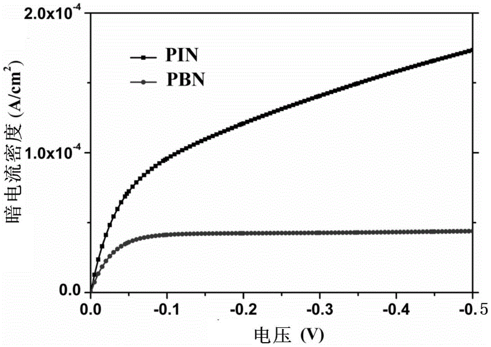
[0028] A PBN-type InGaAs infrared detector with a cut-off wavelength of 2.6μm is structured as follows: a thickness of 1μm and a Si doping concentration of 2×10 are sequentially grown on an n-type InP substrate 18 cm -3 N-type InAs 0.60 P 0.40 Buffer layer, continue to grow with a thickness of 3μm and Si doping concentration of 8×10 16 cm -3 In 0.82 Ga 0.18 As absorption layer, the thickness of the re-growth is 200nm, and the Si doping concentration is 2×10 16 cm -3 In 0.82 Al 0.18 As barrier layer, the final growth thickness is 100nm, Be doping concentration is 2×10 17 cm -3 P-type In 0.82 Ga 0.18 The As window layer forms the PBN detector structure.

[0029] The manufacturing method of the above PBN-type InGaAs infrared detector can firstly grow Si-doped InAs on the InP substrate using the MOCVD system on the n-type InP substrate. 0.60 P 0.40 Buffer layer, that is, the first step is to grow a layer of InAs with a thickness of 100nm at a temperature of 450℃ 0.60 P 0.40 , And then i...


PUM


Abstract

The invention discloses a PBN type InGaAs infrared detector, which belongs to the technical field of optoelectronic materials and devices. The technical problem that the InGaAs detector has more dark currents in the prior art is solved, and the response range of the InGaAs detector is further improved. The infrared detector is composed of a window layer, a blocking layer, an absorbing layer, a buffer layer and a substrate arranged sequentially from top to bottom, wherein the material of the blocking layer has a band gap greater than that of the absorbing layer and the window layer, And the Si-doped InAlAs material or the Si-doped InAsP material whose crystal lattice matches the absorption layer, the thickness of the barrier layer is 100-300 nm. The infrared detector can well suppress the generation of dark current, has high quantum efficiency, low surface recombination and wider response range, and can be used for remote sensing detection.

Description

Technical field [0001] The invention belongs to the technical field of optoelectronic materials and devices, and specifically relates to a PBN-type InGaAs infrared detector. Background technique [0002] Photoelectric detectors are the core of aerospace remote sensing instruments, restricting the level and development of aerospace optical remote sensing instruments. Because the detector made of InGaAs material has the advantages of high sensitivity, fast response speed, good anti-radiation characteristics, and room temperature operation, it becomes an ideal material for space remote sensing in the near-infrared band. At present, the PIN structure is adopted in the detector structure design, especially in the semiconductor photovoltaic infrared detector. However, with the rapid development of material preparation technology and device structure design, people are eager to develop new infrared detectors to improve the performance of the current photodetector devices in terms of th...

Claims


Application Information

Patent Timeline
Patent Type & Authority Patents(China)
IPC IPC(8): H01L31/0304H01L31/101
CPCH01L31/03046H01L31/101
Inventor 张志伟缪国庆宋航蒋红李志明黎大兵孙晓娟陈一仁
Owner CHANGCHUN INST OF OPTICS FINE MECHANICS & PHYSICS CHINESE ACAD OF SCI
Why Eureka
Try Eureka