Flip chip failure analysis method and preparation method of detection sample in electric property positioning

A technology for failure analysis and sample detection, which is applied in the testing/measurement of circuits, electrical components, semiconductors/solid-state devices, etc. It can solve the problems that gold bumps cannot be packaged and re-wired, and the failure analysis that affects the positioning of electrical bright spots, etc., to achieve Avoid the effect of being corroded

Active Publication Date: 2015-12-30
INTEGRA TED SERVICE TECH SHANGHAI CO LTD
View PDF8 Cites 14 Cited by
  • Summary
  • Abstract
  • Description
  • Claims
  • Application Information

AI Technical Summary

Problems solved by technology

like figure 2 As shown, the current method is: first use grinding method to grind off the solder ball 95 and 2/3 of the packaging substrate 91, and then use an acid solution to remove the plastic package 93 outside the 92 and connect the die 92 and 1/3 of the packaging substrate 91 Separate the chip 90 and take the bare chip 92, then paste the back of the bare chip 92 on the transparent glass substrate 96 through transparent colloid (red glue), and finally connect the conductive sheet 98 on the glass substrate 96 thr

Method used


Image

  • Flip chip failure analysis method and preparation method of detection sample in electric property positioning
  • Flip chip failure analysis method and preparation method of detection sample in electric property positioning
  • Flip chip failure analysis method and preparation method of detection sample in electric property positioning

Examples


preparation example Construction

[0054] Cooperate with reference Figure 4 ~ Figure 7 as shown, Figure 4 It is a flow chart of the preparation method of the detection sample in the electrical positioning of the failure analysis of the flip-chip chip. Figure 5 ~ Figure 7 It is an exploded view of the steps of the preparation method of the detection sample in the electrical positioning of the failure analysis of the flip-chip chip of the present invention. The preparation method of the flip-chip chip failure analysis and detection sample of the present invention comprises:

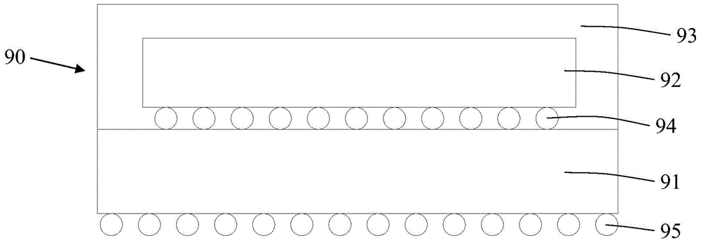
[0055] Step S101 : combine Figure 5 As shown, a flip chip 10 to be tested is provided. The flip chip 10 includes a package substrate 11 and a die 12 prepared on the package substrate 11. The outside of the die 12 is covered with a plastic package 13. The die 12 and the package substrate 11 Gold bumps 14 are connected between them, and solder balls 15 are welded on the bottom of the packaging substrate 11 . The packaging substrate 1...


PUM


Abstract

The invention discloses a flip chip failure analysis method and a preparation method of a detection sample in electric property positioning. The preparation method includes the steps that a flip chip to be detected is provided, wherein the flip chip comprises a packaging substrate and a bare chip prepared on the packaging substrate, the bare chip is covered with a plastic package body, a gold bump is connected between the bare chip and the packaging substrate, and a solder ball is welded to the bottom of the packaging substrate; the plastic package body outside the bare chip is ground till the crystal back of the bare chip is exposed; the back face of the bare chip is combined to a glass base plate, and a conducting strip is arranged on the glass base plate; the conducting strip on the glass base plate is electrically connected with the solder ball at the bottom of the packaging substrate through a packaging binding wire, and then the detection sample is obtained. According to the preparation method of the detection sample for flip chip failure analysis, the plastic package body on the back face of the bare chip is ground away, then the back face of the bare chip is combined on the glass base plate for failure analysis, the plastic package body does not need to be corroded, the packaging substrate and the bare chip do not need to be separated, and therefore the probability that the gold bump is corroded in the bare chip taking process is avoided.

Description

technical field [0001] The invention relates to the technical field of semiconductors, in particular to a flip-chip chip failure analysis method and a method for preparing detection samples in electrical positioning. Background technique [0002] Due to the rapid development of semiconductor technology, chips with high-end 28nm or even smaller technology have been widely used at home and abroad. The general packaging form can no longer meet the requirements of the chip transmission rate, and the emergence of flip-packaging technology has solved this problem. At present, flip-packaged chips have been widely used in various fields, and advanced packaging such as C4 packaging will become the mainstream in the future. [0003] Because flip-package chips usually have more metal layers, and there are solder balls on the front side. Therefore, usually the bright spots may be blocked by metal and tin balls, so that abnormal bright spots cannot be accurately located. to combine F...

Claims


Application Information

Patent Timeline
IPC IPC(8): H01L21/66
CPCH01L22/12
Inventor 李鹏云刘国庆葛金发曾元宏
Owner INTEGRA TED SERVICE TECH SHANGHAI CO LTD
Why Eureka
Try Eureka