Semiconductor Laser Device

Inactive Publication Date: 2007-12-27
HAMAMATSU PHOTONICS KK
View PDF3 Cites 12 Cited by
  • Summary
  • Abstract
  • Description
  • Claims
  • Application Information

AI Technical Summary

Benefits of technology

[0018] In accordance with the present invention, a semiconductor laser apparatus having a metal body for efficiently cooling a semiconductor device, in which joining of copper-made

Problems solved by technology

However, the lowering in conductivity (that is, an increase in resistance) increases the activity of the fluid, so that the corrosiveness due to the volume reduction of the metal body increases inversely.
In addition, the device for lowering the conductivity becomes large in size and high in cost, so that the lowering

Method used


Image

  • Semiconductor Laser Device
  • Semiconductor Laser Device
  • Semiconductor Laser Device

Examples


Example

First Embodiment

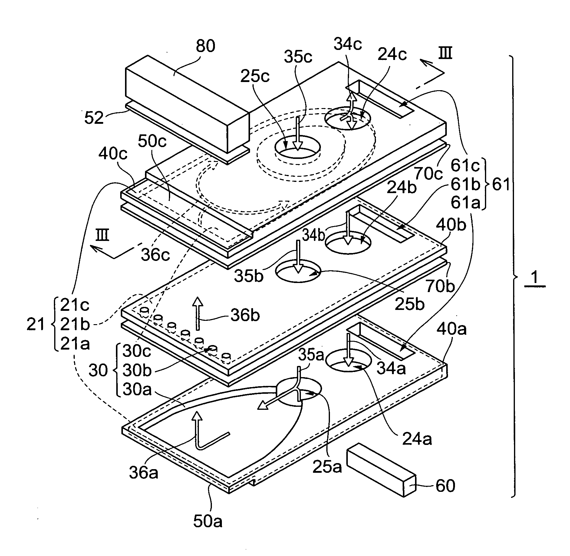
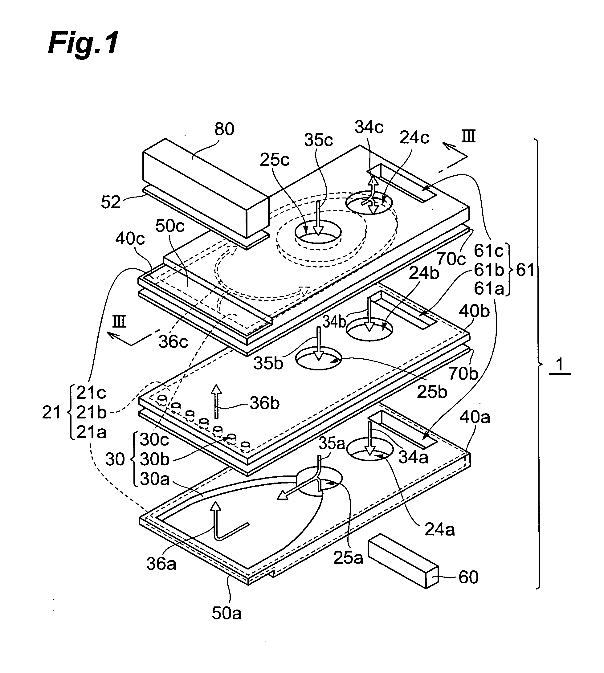
[0033] First, a first embodiment of the semiconductor laser apparatus according to the present invention will be explained. FIG. 1 is an exploded perspective view showing a construction of a semiconductor laser apparatus 1 according to the first embodiment.

[0034] The semiconductor laser apparatus 1 comprises a metal body 21, adhesives 70b and 70c, DLC layers (diamond-like carbon layers) 40a, 40b, and 40c, and a semiconductor laser element 80.

[0035] The metal body 21 is formed by bonding a first copper-made member 21a, a second copper-made member 21b, and a third copper-made member 21c, and is provided with a fluid channel 30 inside. The metal body 21 has a penetrating conductor 60 which penetrates the metal body 21 in a region in which the fluid channel 30 is not formed, and a housing hole 61 for housing the penetrating conductor 60. The housing hole 61 consists of three conductor holes 61a, 61b, and 61c. On the metal body 21, exposed regions 50a and 50c are set. ...
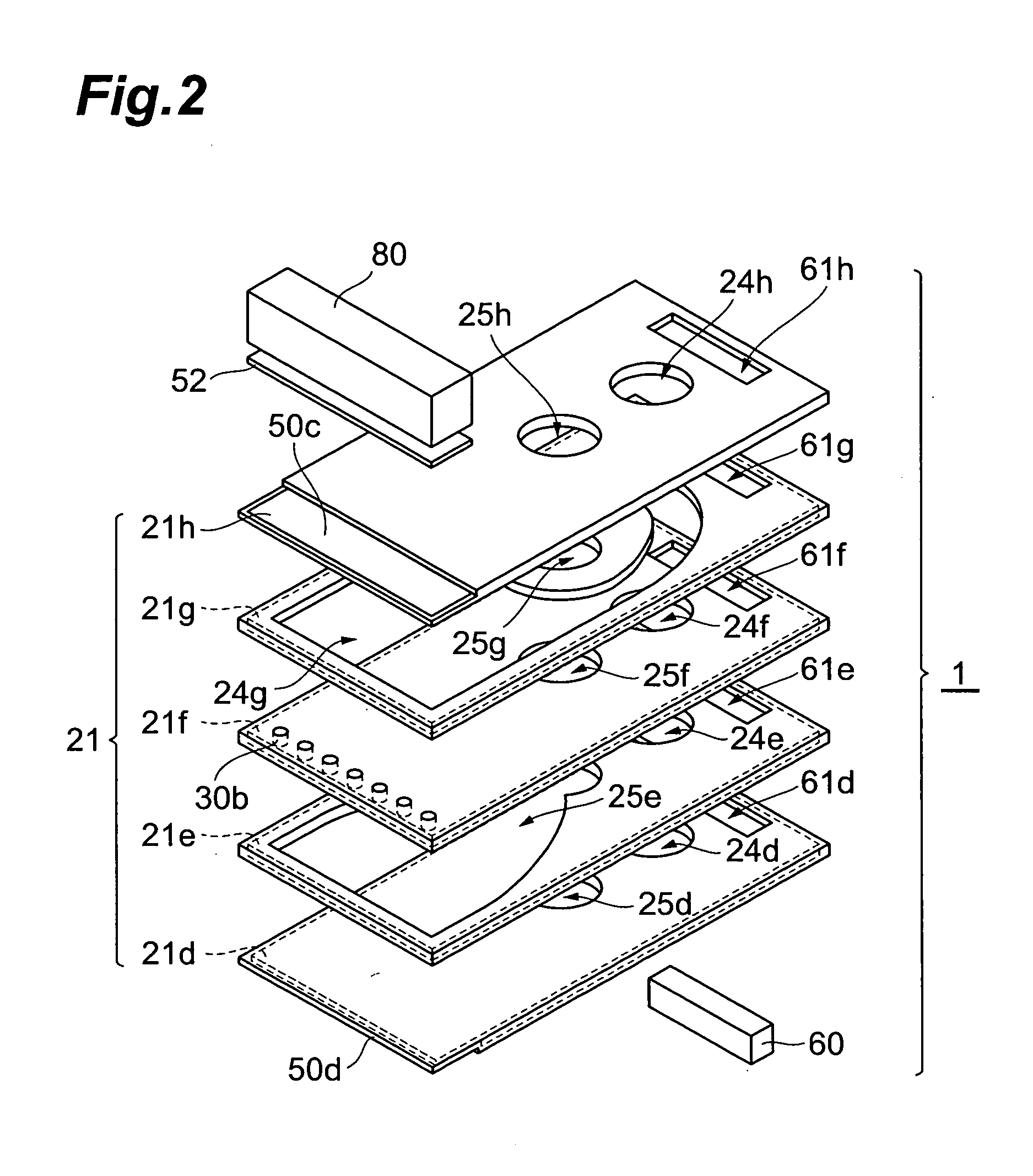
Example

Second Embodiment

[0074] Next, a second embodiment of the semiconductor laser apparatus according to the present invention will be explained. FIG. 9 is a perspective view showing a construction of a semiconductor laser apparatus 2 according to the second embodiment.

[0075] The semiconductor laser apparatus 2 includes, in addition to the semiconductor laser element 80 and the metal body 21, an n-side electrode 81 on the semiconductor laser element 80, a dummy spacer 82 filled between the n-side electrode 81 and the metal body 21, and silicon rubber 83 for sealing on the metal body 21. An O-ring may be applied instead of the silicon rubber 83 for sealing.

[0076] The metal body 21 includes, as shown in FIG. 9, two columnar penetrating conductors 60X and 60Y which penetrate the metal body 21 while avoiding the fluid channel. The penetrating conductors 60X and 60Y are housed in housing holes 61X and 61Y formed in the metal body 21. The inner wall faces of the housing holes 61X and 61Y ar...


PUM


Abstract

The present invention relates to a semiconductor laser apparatus having a metal body which efficiently cools a semiconductor laser element, in which joining of copper-made members coated with DLC layers and prevention of corrosion in the vicinity of joined portions are possible. The semiconductor laser apparatus has a metal body as a heat sink for cooling the semiconductor laser element. The metal body is constituted by a plurality of copper-made members, and the surfaces of each copper-made members are continuously coated with a diamond carbon layer except for regions corresponding to an exposed region in which the semiconductor laser element is mounted.

Description

TECHNICAL FIELD [0001] The present invention relates to a semiconductor laser apparatus which has a semiconductor laser element as a light emitting source and has a structure for efficiently cooling this semiconductor laser device. BACKGROUND ART [0002] As a heat sink essential for cooling a heating element such as a semiconductor laser element with a high output, a metal body which is constituted by joining a plurality of metal members such as copper-made members and has a structure for circulating a fluid for cooling a heating element in a fluid channel provided inside, is known. [0003] For cooling a semiconductor laser element, normally, a construction in which a plurality of metal bodies are stacked so as to sandwich the semiconductor laser element is employed. In this case, each metal body not only cools each semiconductor laser element but also serves as an electrical conduction path among semiconductor laser elements, so that an electrical potential difference occurs between ...

Claims


Application Information

Patent Timeline
IPC IPC(8): H01S3/16H01S5/023
CPCH01L24/83H01L2224/83801H01S5/02236H01L2924/01079H01S5/02423H01S5/405H01L2924/01068H01S5/02272H01S5/0237H01S5/023H01S5/0233H01S5/0235
Inventor MIYAJIMA, HIROFUMIKAN, HIROFUMI
Owner HAMAMATSU PHOTONICS KK
Why Eureka
Try Eureka