Adjustable hybrid imaging detector pixel structure and preparation method thereof

An imaging detector and pixel structure technology, applied in the field of microelectronics, can solve the problems of large alignment deviation of the infrared image part and the visible light image part, affecting the imaging quality, etc., so as to reduce the size and cost of the device and improve the imaging quality. Effect

Active Publication Date: 2015-12-30
SHANGHAI INTEGRATED CIRCUIT RES & DEV CENT
View PDF4 Cites 5 Cited by
  • Summary
  • Abstract
  • Description
  • Claims
  • Application Information

AI Technical Summary

Problems solved by technology

[0003] However, in the existing hybrid imaging devices, lenses are used to form two optical paths to sense and image visible light and infrared light respectively, and finally a computer processing system is used to

Method used


Image

  • Adjustable hybrid imaging detector pixel structure and preparation method thereof
  • Adjustable hybrid imaging detector pixel structure and preparation method thereof
  • Adjustable hybrid imaging detector pixel structure and preparation method thereof

Examples


Embodiment Construction

[0054] In order to make the content of the present invention clearer and easier to understand, the content of the present invention will be further described below in conjunction with the accompanying drawings. Of course, the present invention is not limited to this specific embodiment, and general replacements known to those skilled in the art are also covered within the protection scope of the present invention.

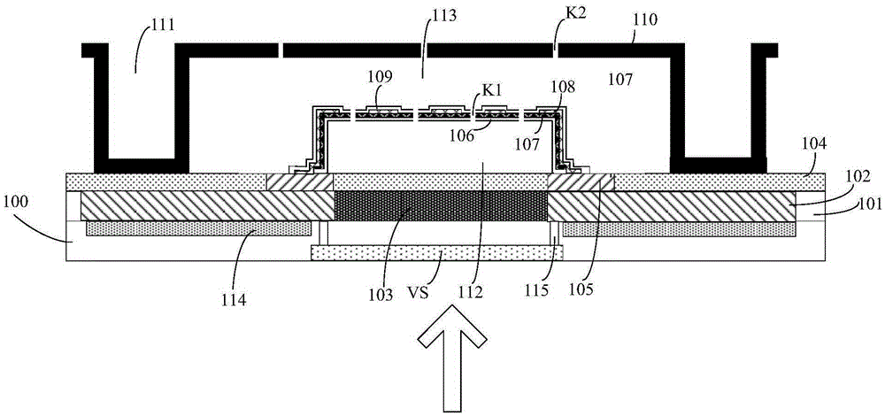
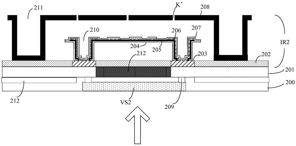
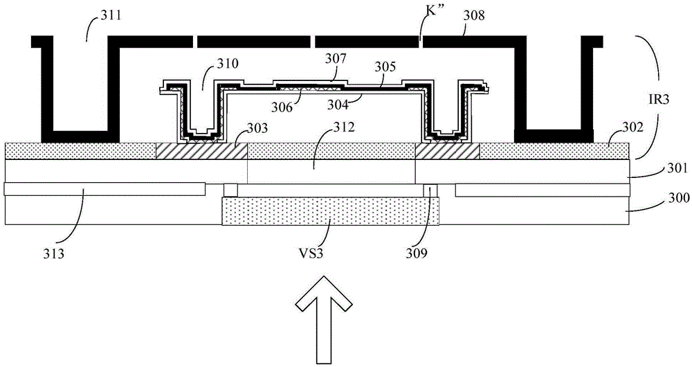
[0055] The pixel structure of the visible light and infrared hybrid imaging detector of the present invention includes: a semiconductor substrate as a visible light filter layer; a visible light sensing area located on the lower surface of the semiconductor substrate, the visible light sensing area includes a visible light sensing component and an extraction pole; located on the semiconductor substrate The infrared sensing area on the surface, which includes: an infrared window material located on the upper surface of the semiconductor substrate, which is used to se...


PUM


Abstract

The invention provides an adjustable hybrid imaging detector pixel structure and a preparation method thereof. According to the adjustable hybrid imaging detector pixel structure and the preparation method thereof of the invention, a visible light induction region and an infrared induction region are integrated in a chip; the infrared induction region includes an infrared window material which is located at the upper surface of a semiconductor substrate and is used for selectively transmitting infrared light of desired bands, interconnection layers which are arranged at two sides of the infrared window material and are located at the upper surface of the semiconductor substrate, a dielectric layer which is located at the upper surfaces of the infrared window material and the interconnection layers, an infrared induction structure which is provided with a first middle arching part and first end portion supporting parts, and a supporting component which is arranged around the infrared induction structure; contact trench structures located at two sides above the infrared window material are formed in the dielectric layer; the first middle arching part is located a corresponding position just above the infrared window material; a first cavity is formed between the first middle arching part and the dielectric layer; and the electrode layers of the first end portion supporting parts contact with the contact trench structures.

Description

technical field [0001] The invention relates to the field of microelectronic technology, in particular to a pixel structure and a preparation method of a visible-infrared hybrid imaging detector whose incident light can be adjusted. Background technique [0002] With the development of industry and living standards, pure infrared imaging or pure visible light imaging can no longer meet the demand. Imaging technologies with wider wavelength bands have attracted more and more attention, especially imaging technologies that are sensitive to visible light and infrared light at the same time. [0003] However, in existing hybrid imaging devices, lenses are used to form two optical paths to sense and image visible light and infrared light respectively, and finally a computer processing system is used to synthesize them together. Due to the separation of the optical paths, the formed infrared image part and visible light image Some of them have large alignment deviations, which ser...

Claims


Application Information

Patent Timeline
IPC IPC(8): H01L27/146
Inventor 康晓旭
Owner SHANGHAI INTEGRATED CIRCUIT RES & DEV CENT
Why Eureka
Try Eureka