Transparent display panel and manufacturing method thereof

A technology for transparent display panels and manufacturing methods, applied in semiconductor/solid-state device manufacturing, electrical components, electric solid-state devices, etc., can solve problems affecting the alignment accuracy of metal mask plates in the production of transparent display panels, etc., to increase service life, The effect of saving production cost and reducing usage

Inactive Publication Date: 2015-12-30
EVERDISPLAY OPTRONICS (SHANGHAI) CO LTD
View PDF5 Cites 15 Cited by
  • Summary
  • Abstract
  • Description
  • Claims
  • Application Information

AI Technical Summary

Problems solved by technology

[0006] Aiming at the defects in the prior art, the purpose of the present invention is to provide a transparent display panel and its manufacturing method, which can effectively solve the problems caused by the metal mask in the cathode manufacturing process of the existing transparent display panel. The deformation of the diaphragm and the blockage of the opening affect the alignment accuracy of the metal mask and the production of the transparent display panel.

Method used


Image

  • Transparent display panel and manufacturing method thereof
  • Transparent display panel and manufacturing method thereof
  • Transparent display panel and manufacturing method thereof

Examples


Embodiment Construction

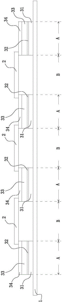
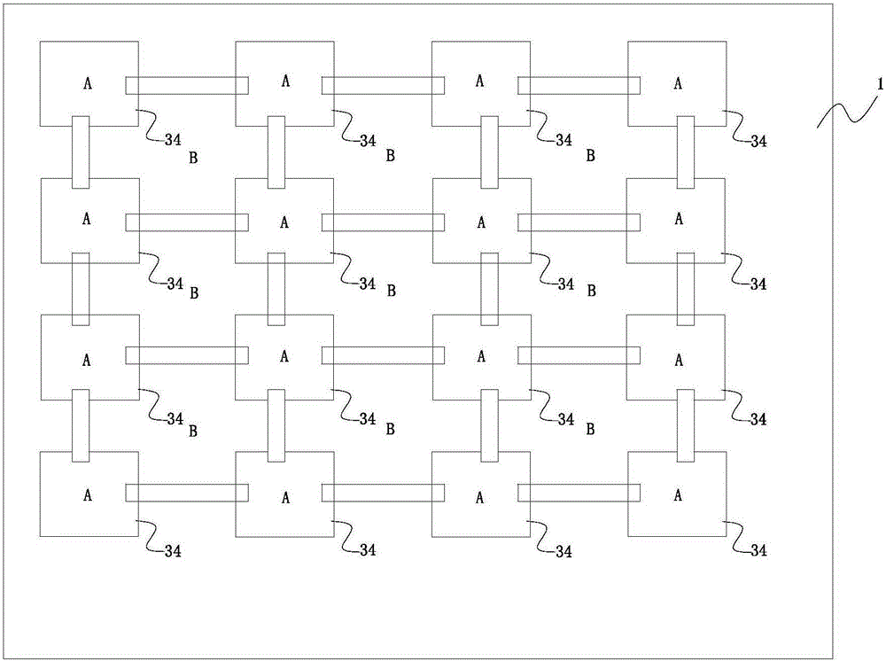
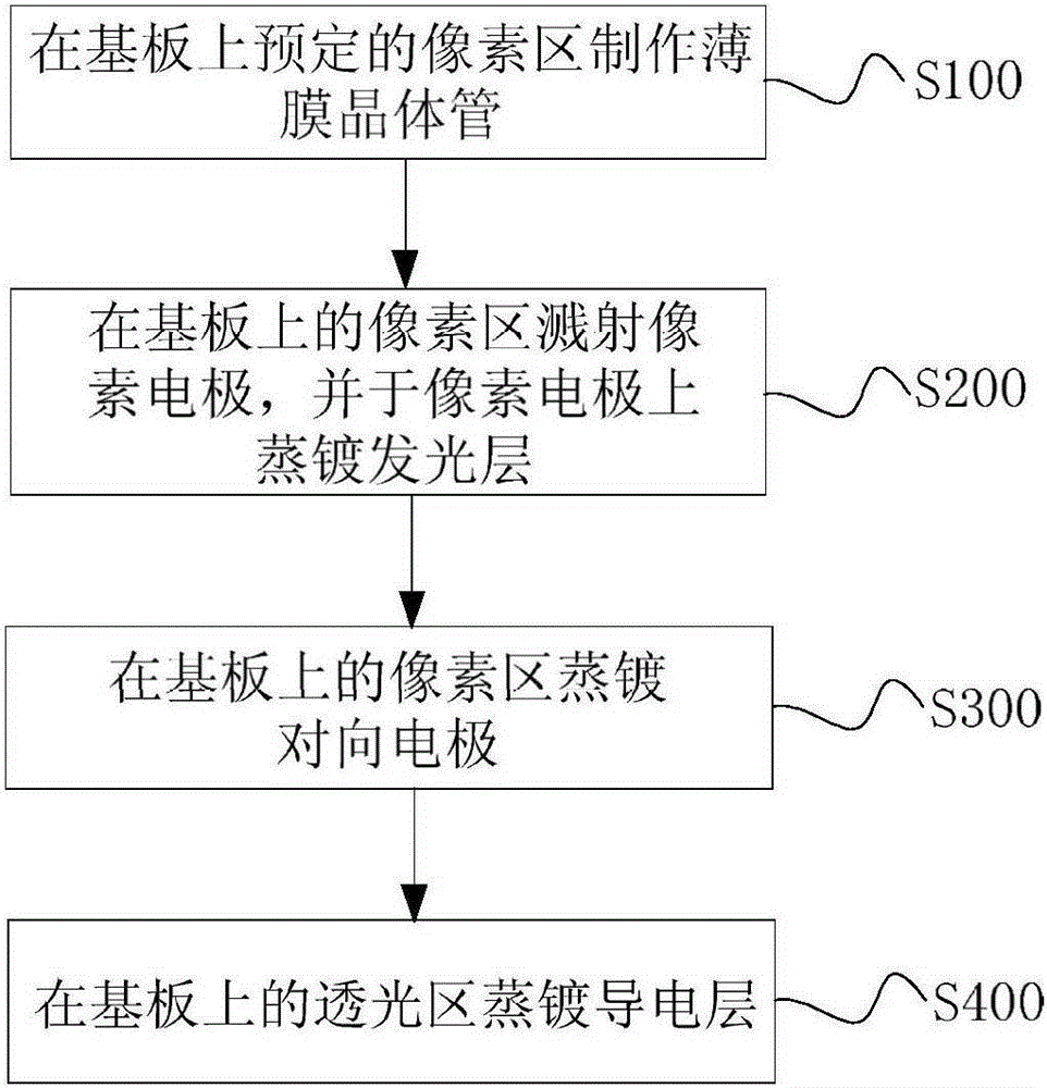
[0032] According to the gist of the present invention, the transparent display panel includes: a substrate including a plurality of pixel regions and a light-transmitting region surrounding the pixel regions; an organic electroluminescence device disposed on the substrate and corresponding to In the pixel region of the substrate, the organic electroluminescent device includes: a thin film transistor disposed on the pixel region of the substrate; a pixel electrode disposed on the thin film transistor and electrically connected to the thin film transistor; a light emitting layer , arranged on the pixel electrode; the counter electrode, arranged in the pixel area of ​​the substrate, and located above the light-emitting layer; a conductive layer, arranged above the light-transmitting area, located in two adjacent Two adjacent opposite electrodes are connected between the opposite electrodes, wherein the conductive layer is made of a conductive material whose evaporation temperature...


PUM


Abstract

The invention discloses a transparent display panel and a manufacturing method thereof. The transparent display panel comprises a substrate, organic electroluminescent devices, pixel electrodes, light-emitting layers, opposite-direction electrodes and a conductive layer, wherein the substrate comprises a plurality of pixel areas and a light transmitting area surrounding the pixel area; the organic electroluminescent devices are arranged on the substrate, correspond to the pixel areas of the substrate and comprise thin film transistors which are arranged on the pixel areas of the substrate; the pixel electrodes are arranged on the thin film transistors and electrically connected with the thin film transistors; the light-emitting layers are arranged on the pixel electrodes; the opposite-direction electrodes are arranged in the pixel areas of the substrate and located above the light-emitting layers; the conductive layer is arranged above the light transmitting area, located between the two opposite-direction electrodes and used for connecting the two adjacent opposite-direction electrodes; the conductive layer is made from conductive materials with the evaporation temperature lower than 600 DEG C.

Description

technical field [0001] The invention relates to the field of designing semiconductor devices, in particular to a transparent display panel and a manufacturing method thereof. Background technique [0002] According to the market research firm IHS, the market value of transparent displays can reach US$100 million in 2015, and will jump to US$87 billion in ten years, with an annual growth rate of nearly twice. Its application fields include many aspects, such as: personal applications (watches, mobile phones, tablet computers, notebook computers, etc.); household appliance displays (refrigerators, microwave ovens, etc.), TV / large-screen displays; advertising displays, office displays, education, Architecture (windows); military use; head-up displays (cars, airplanes), etc. [0003] One of the main indicators of transparent display is its transparency (that is, light transmittance). Compared with many display panels, OLED panels have become the development of transparent displ...

Claims


Application Information

Patent Timeline
Patent Type & Authority Applications(China)
IPC IPC(8): H01L27/32H01L51/52H01L51/56
Inventor 李艳虎余磊
Owner EVERDISPLAY OPTRONICS (SHANGHAI) CO LTD
Why Eureka
Try Eureka