Pixel compensation circuit

A technology for compensating circuits and pixels, applied in the field of electronics, can solve the problems of affecting display quality, increasing the difficulty of the process, uneven brightness of the panel, etc., to reduce the risk of challenging the process capability, reduce the pixel resistance and capacitance load, and change the layout and wiring space. big effect

Active Publication Date: 2016-01-06
EVERDISPLAY OPTRONICS (SHANGHAI) CO LTD
View PDF8 Cites 4 Cited by
  • Summary
  • Abstract
  • Description
  • Claims
  • Application Information

AI Technical Summary

Problems solved by technology

Among them, the active organic light emitting diode (Active matrix OLED, AMOLED) has received more attention due to its advantages of large size and high resolution. However, the change of the critical voltage of the existing active organic light emitting diode will cause the OLED to The current is different, resulting in uneven brightness of the panel, affecting the display quality, and the phenomenon of material aging with long-term use will also affect the display quality
[0003] In the prior art, there are various pixel compensation circuits for compensating the threshold voltage change of thin film transistors to realize the compensation for the threshold voltage change. However, most of the pixel compensation circuits in the prior art are designed to use P-type thin film transistors (TFTs) for compensation. circuit, and the component design using multiple thin film transistors in the pixel has almost filled the pixel space on the array circuit, causing the layout and wiring space of other lines in the pixel (Pixel) to be compressed, not only causing the aperture ratio (ApertureRatio ) is too low, which will affect the luminous efficiency, and will also increase the difficulty of the process, as well as the resistance-capacitance load (RCloading)

Method used


Image

  • Pixel compensation circuit
  • Pixel compensation circuit
  • Pixel compensation circuit

Examples


Embodiment Construction

[0040] The following will clearly and completely describe the technical solutions in the embodiments of the present invention with reference to the accompanying drawings in the embodiments of the present invention. Obviously, the described embodiments are only some, not all, embodiments of the present invention. Based on the embodiments of the present invention, all other embodiments obtained by persons of ordinary skill in the art without creative efforts fall within the protection scope of the present invention.

[0041] It should be noted that, in the case of no conflict, the embodiments of the present invention and the features in the embodiments can be combined with each other.

[0042] The present invention will be further described below in conjunction with the accompanying drawings and specific embodiments, but not as a limitation of the present invention.

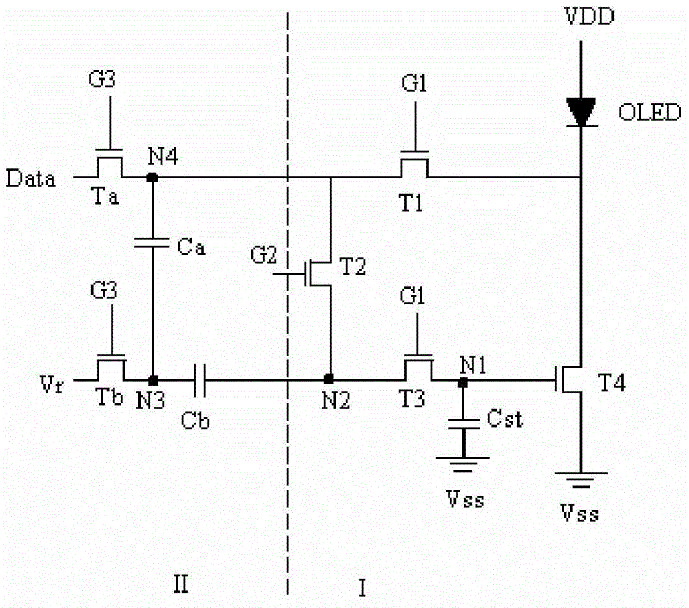
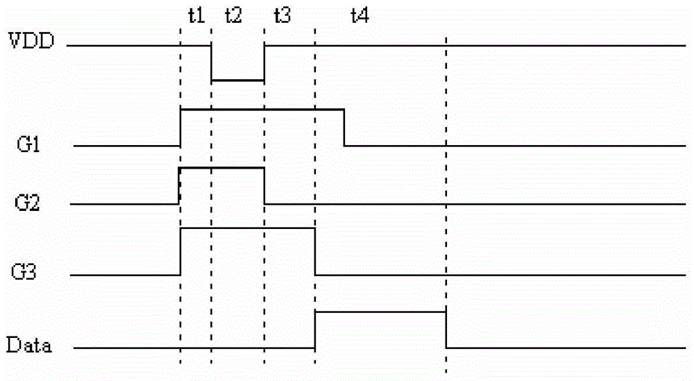
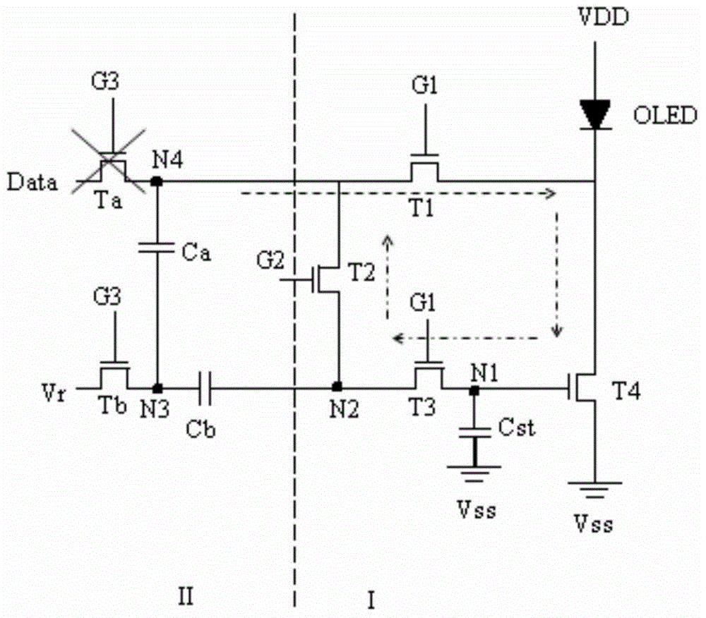
[0043] refer to figure 1 , a pixel compensation circuit, including:

[0044] A light-emitting device OLED, con...


PUM


Abstract

The present invention concretely discloses a pixel compensation circuit. The pixel compensation circuit comprises a luminescent device emitting light under the action of a drive signal; a drive transistor producing the drive signal under the action of data voltage; a first voltage storage unit used for storing the data voltage; and a data voltage end for switchably writing the data voltage into a grid electrode of the drive transistor through a coupling capacitor, wherein the luminescent device, the first voltage storage unit and the drive transistor are disposed at a first pixel inner region. The pixel compensation circuit provided by the present invention has a voltage compensating effect on the drive transistor, extra current is produced meanwhile to carry out extra compensation on the situation of crossed voltage rise caused by long-time usage of an OLED assembly, the circuit is divided into pixel inner and outer regions, an aperture opening ratio of the pixel inner region is raised, locating and wiring space of the pixel inner region is enlarged, and technical risks and pixel resistance-capacitance loads are lowered.

Description

technical field [0001] The invention relates to the field of electronic technology, in particular to a pixel compensation circuit. Background technique [0002] In the development of display technology, organic light-emitting diode displays have a series of advantages such as thinness, flexibility, fast response time and wide viewing angle, and are considered to be the most promising display technology. Among them, the active organic light emitting diode (Active matrix OLED, AMOLED) has received more attention due to its advantages of large size and high resolution. However, the change of the critical voltage of the existing active organic light emitting diode will cause the OLED to The current is different, resulting in uneven brightness of the panel, which affects the display quality, and the phenomenon of material aging occurs with long-term use, which will also affect the display quality. [0003] In the prior art, there are various pixel compensation circuits for compe...

Claims


Application Information

Patent Timeline
Patent Type & Authority Applications(China)
IPC IPC(8): G09G3/3233
Inventor 张玮轩
Owner EVERDISPLAY OPTRONICS (SHANGHAI) CO LTD
Why Eureka
Try Eureka