Fan-out type packaging structure and manufacturing method thereof

A technology of packaging structure and manufacturing method, applied in semiconductor/solid-state device manufacturing, electrical components, electric solid-state devices, etc., can solve the problems of low yield rate and high packaging cost, so as to improve yield rate, save materials, avoid thinning and The effect of the laser drilling process

Active Publication Date: 2016-01-06
SJ SEMICON JIANGYIN CORP
View PDF5 Cites 33 Cited by
  • Summary
  • Abstract
  • Description
  • Claims
  • Application Information

AI Technical Summary

Problems solved by technology

[0007] In view of the shortcomings of the prior art described above, the purpose of the present invention is to provide a fan-out packa

Method used


Image

  • Fan-out type packaging structure and manufacturing method thereof
  • Fan-out type packaging structure and manufacturing method thereof
  • Fan-out type packaging structure and manufacturing method thereof

Examples


Embodiment 1

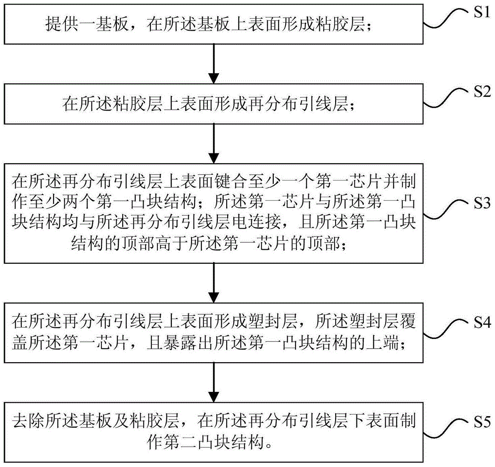
[0078] The present invention provides a method for manufacturing a fan-out packaging structure, please refer to figure 1 , shown as a process flow diagram of the method, comprising the following steps:

[0079] S1: providing a substrate, forming an adhesive layer on the upper surface of the substrate;

[0080] S2: forming a redistribution lead layer on the upper surface of the adhesive layer;

[0081] S3: bonding at least one first chip on the upper surface of the redistribution wiring layer and fabricating at least two first bump structures; both the first chip and the first bump structure are connected to the redistribution wiring layer electrically connected, and the top of the first bump structure is higher than the top of the first chip;

[0082] S4: forming a plastic sealing layer on the upper surface of the redistribution lead layer, the plastic sealing layer covers the first chip and exposes the upper end of the first bump structure;

[0083] S5: removing the substr...

Embodiment 2

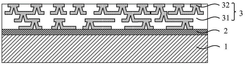
[0115] The present invention also provides a fan-out packaging structure, such as Figure 12 As shown, it is a schematic diagram of the fan-out package structure, including:

[0116] Redistribute lead layer 3;

[0117] At least one first chip 4 bonded to the upper surface of the redistribution wiring layer 3 and electrically connected to the redistribution wiring layer 3;

[0118] At least two first bump structures 5 that are electrically connected to the redistribution lead layer 3 and whose tops are higher than the first chip 4;

[0119] Covering the first chip 4 and exposing the plastic sealing layer 6 on the upper end of the first bump structure 5;

[0120] And the second bump structure 7 fabricated on the lower surface of the redistribution lead layer 3 .

[0121] Specifically, the redistribution lead layer 3 includes a dielectric layer 31 and at least one layer of redistribution metal lines 32 formed in the dielectric layer 31 . As an example, the redistribution lead...


PUM


Abstract

The invention provides a fan-out type packaging structure and a manufacturing method thereof. The method includes the steps of: S1. providing a substrate, and forming an adhesive layer on an upper surface of the substrate; S2. forming a redistribution lead layer on an upper surface of the adhesive layer; S3. bonding at least one first chip and manufacturing at least two first lug structures on an upper surface of the redistribution lead layer, wherein the first chips and the first lug structures are electrically connected with the redistribution lead layer, and the tops of the first lug structures are higher than the tops of the first chips; S4. forming a plastic packaging layer on the upper surface of the redistribution lead layer, the plastic packaging layer covering the first chips and exposing upper ends of the first lug structures; and S5. removing the substrate and the adhesive layer, and manufacturing second lug structures on a lower surface of the redistribution lead layer. The manufacturing method of the fan-out type packaging structure can reduce offset between the chips and the redistribution lead layer, thereby improving the yield; and a packaging process is relatively simple, and product cost can be reduced.

Description

technical field [0001] The invention belongs to the field of semiconductor packaging, and relates to a fan-out packaging structure and a manufacturing method thereof. Background technique [0002] The semiconductor industry continues to increase the integration density of various electronic components by continuously reducing the minimum feature size, so that more electronic components can be integrated in a given area. At present, the most advanced packaging solutions include wafer-level chip-scale packaging (Waferlevelchip-scalepackage), fan-out wafer-level packaging (Fan-outwaferlevelpackage), flip-chip (Flipchip), and stacked packaging (PackageonPackage, POP), etc. . [0003] Traditional fan-out wafer-level packaging (Fan-out wafer level packaging, FOWLP) generally includes the following steps: first cut a single microchip from the wafer, and use standard pick-and-place equipment to stick the chip face-down to the adhesive of the carrier. layer; then form a plastic sea...

Claims


Application Information

Patent Timeline
IPC IPC(8): H01L21/48H01L23/488H01L23/498H01L21/60
CPCH01L21/4846H01L23/498H01L24/11H01L24/81H01L2224/11H01L2224/81H01L2924/181H01L2224/48091H01L23/3128H01L21/568H01L21/6835H01L2221/68345H01L2224/32145H01L2224/81005H01L2924/15192H01L2924/15311H01L2924/1533H01L23/5384H01L23/5389H01L24/97H01L25/0655H01L25/105H01L24/13H01L24/16H01L2224/16227H01L2224/48227H01L24/48H01L2224/131H01L2225/1023H01L2225/1058H01L2225/0651H01L2225/06568H01L2924/00012H01L2924/00014H01L2924/014H01L2224/16225H01L23/488H01L21/48H01L25/065H01L21/56H01L2224/02379H01L2224/04105H01L2224/12105H01L2224/81801
Inventor 林正忠蔡奇风
Owner SJ SEMICON JIANGYIN CORP
Why Eureka
Try Eureka