

Organic electroluminescent device, preparation method thereof and display device
An electroluminescence device and electroluminescence technology, which are applied in the directions of organic light-emitting devices, organic light-emitting device parameters, organic semiconductor devices, etc., can solve the problems of reduced luminous efficiency and lifespan of light-emitting devices, different numbers of electrons and holes, etc. The effect of improving luminous efficiency and lifespan
- Summary
- Abstract
- Description
- Claims
- Application Information
AI Technical Summary
Problems solved by technology
Method used
Image

Examples
Embodiment 1
[0065] This embodiment provides an organic electroluminescence device, an anode layer, a cathode layer, and a light-emitting layer disposed between the anode layer and the cathode layer; wherein, between at least one of the anode layer and the cathode layer and the light-emitting layer There is a carrier rate adjustment layer; the carrier rate adjustment layer is used to adjust the injection rate of carriers.
[0066] When driving organic electroluminescent devices to emit light, the injection rate of holes injected into the light-emitting layer from the anode layer is different from that of electrons injected into the light-emitting layer from the cathode layer, that is, the hole injection rate is less than the electron injection rate, which will cause the injection to emit light at the same time. The number of electrons and the number of holes in the layer recombination zone are different, which leads to a decrease in the luminous efficiency and lifetime of the organic electrolu...
Embodiment 2
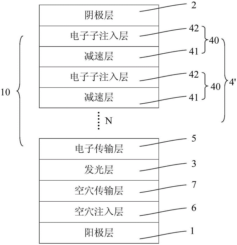
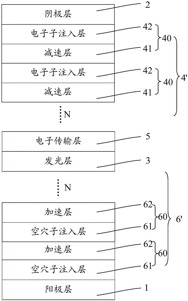
[0068] Such as figure 1 As shown, this embodiment provides an organic electroluminescent device and a preparation method thereof. The organic electroluminescent device includes an anode layer 1, a light-emitting layer 3, a carrier rate adjustment layer 10, and a cathode layer 2. Wherein, the carrier rate adjustment layer 10 in this embodiment at least includes an electron rate adjustment layer 4'; the electron rate adjustment layer 4'includes a plurality of continuously arranged electron trap units 40, and the electron trap unit 40 includes an edge deviation The electron injection layer 42 and the deceleration layer 41 are sequentially arranged in the direction of the cathode layer; the electron injection layer 42 is used to inject electrons into the deceleration layer 41; the deceleration layer 41 is used to slow down the electron injection rate.
[0069] In other words, when the organic electroluminescent device is applied with an external voltage, the electrons injected from th...
Embodiment 3
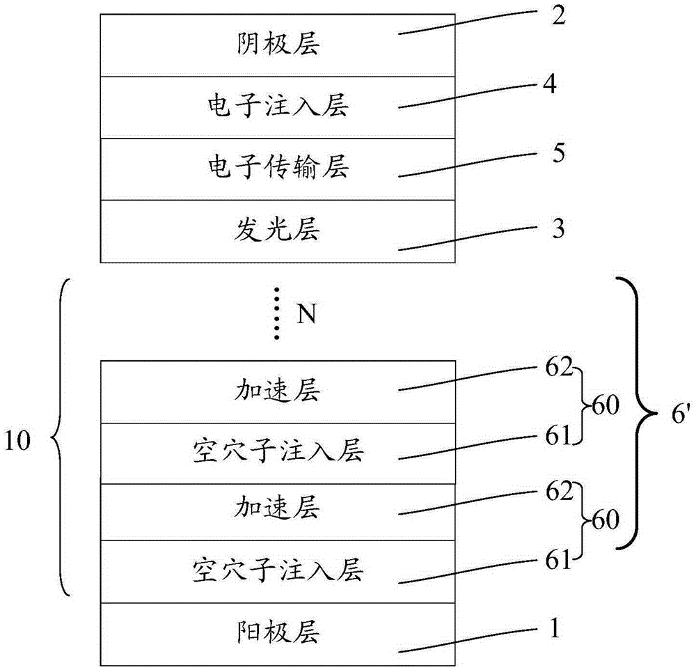
[0095] Such as figure 2 As shown, this embodiment provides an organic electroluminescent device and a preparation method thereof. The organic electroluminescent device includes a substrate, an anode layer 1, a carrier rate adjusting layer 10, and a light emitting layer 3 sequentially disposed on the substrate. And the cathode layer 2. Wherein, the carrier rate adjustment layer 10 in this embodiment includes a hole rate adjustment layer 6'; the hole rate adjustment layer 6'includes a plurality of continuously arranged hole acceleration units 60; each hole acceleration unit 60 It includes a hole injection layer 61 and an acceleration layer 62 that are arranged in a direction away from the anode layer 1; wherein the hole injection layer 61 is used to inject holes into the acceleration layer 62; the acceleration layer 62 is used to increase holes Injection rate.
[0096] In this embodiment, since a carrier rate adjustment layer 10 is added between the anode layer 1 and the light-em...
PUM
| Property | Measurement | Unit |
|---|---|---|
| Electron mobility | aaaaa | aaaaa |
| Thickness | aaaaa | aaaaa |
| Thickness | aaaaa | aaaaa |
Abstract
Description
Claims
Application Information