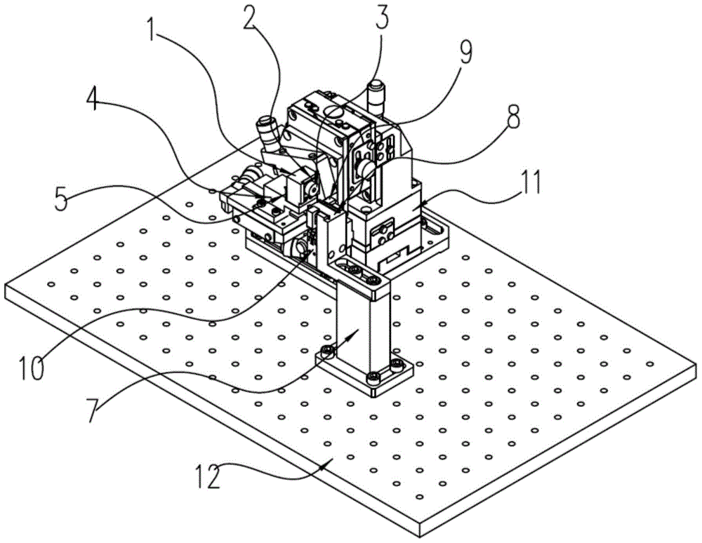
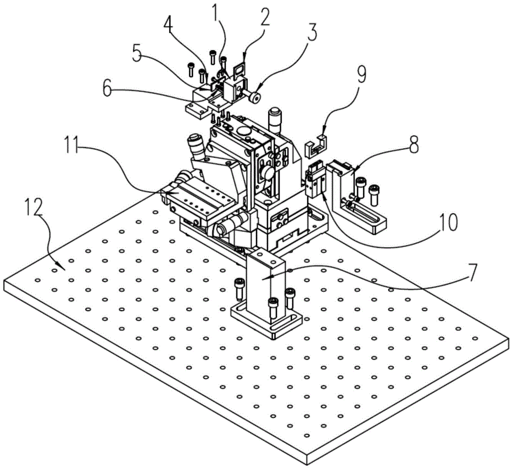
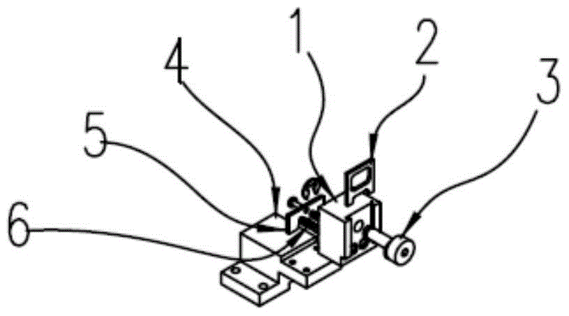
A coupling platform for SFP+COB module components for optoelectronic communication

A technology of photoelectric communication and PCB board, which is applied in the field of optical communication, can solve the problems of no mature coupling assembly process, etc., and achieve the effect of reliable positioning, fast coupling speed and simple process

Active Publication Date: 2017-03-22
WUHAN TELECOMM DEVICES
View PDF6 Cites 0 Cited by
  • Summary
  • Abstract
  • Description
  • Claims
  • Application Information

AI Technical Summary

Problems solved by technology

[0003] The COB (Chip On Board) solution for photoelectric communication modules is a relatively new technology solution. This solution directly couples the lens with the adapter to the PCB board on which the IC chip is mounted and fixes it with glue. There is no mature coupling assembly in the industry. In order to achieve mass production of such modules, a practical and efficient coupling platform must be developed

Method used


Image

  • A coupling platform for SFP+COB module components for optoelectronic communication
  • A coupling platform for SFP+COB module components for optoelectronic communication
  • A coupling platform for SFP+COB module components for optoelectronic communication

Examples


Embodiment Construction

[0034] The present invention will be described in further detail below in conjunction with specific embodiments and accompanying drawings. Examples of the described embodiments are shown in the drawings, wherein like or similar reference numerals designate like or similar elements or elements having the same or similar functions throughout. The embodiments described below with reference to the accompanying drawings are exemplary, and are only used to explain the technical solution of the present invention, and should not be construed as limiting the present invention.

[0035] In the description of the present invention, the terms "inner", "outer", "longitudinal", "transverse", "upper", "lower", "top", "bottom" or "front", "rear", "left ", "right" and other indicated orientations or positional relationships are based on the orientations or positional relationships shown in the drawings, and are only for the convenience of describing the present invention and do not require tha...


PUM


Abstract

The present invention provides a coupling platform for SFP+COB module assembly for photoelectric communication, which includes a lens clamping part, a PCB board clamping part, a coupling adjustment part and a support part, and the lens clamping part includes a clamping seat, a movable part, a cam, Connecting seat, jumper press plate and jumper; PCB board clamping part includes PCB seat, gripper and air claw; the main body of coupling adjustment part is multi-axis fine-tuning frame; The combination of seat, movable part and cam makes the cam drive the movable part to slide up and down in the slot of the clamping seat when the cam rotates. When the movable part runs on the upper end, the LC optical port of the plastic lens can be inserted into the clamping seat without hindrance ;When the movable part runs at the lower end, the LC optical port of the plastic lens is limited by the limit gap of the movable part; The technical problem of positioning the lens and bonding it to the PCB board has achieved good results in improving quality, efficiency and reducing production costs.

Description

technical field [0001] The invention relates to the technical field of optical communication, in particular to providing a coupling platform for SFP+COB module components for optical communication. Background technique [0002] With the development of global optical communication networks, the communication rate continues to increase, and the more cables are replaced by optical fibers, the demand for short-distance optical modules in high-speed miniaturization packages also increases. The increase in demand makes multi-functional and flexible , Low-cost optical communication components have become an inevitable trend of development. [0003] The COB (Chip On Board) solution for photoelectric communication modules is a relatively new technology solution. This solution directly couples the lens with the adapter to the PCB board on which the IC chip is mounted and fixes it with glue. There is no mature coupling assembly in the industry. In order to achieve mass production of s...

Claims


Application Information

Patent Timeline
Patent Type & Authority Patents(China)
IPC IPC(8): G02B6/42
CPCG02B6/4204G02B6/4226G02B6/428G02B6/4287G02B7/02G02B6/4206G02B6/4236G02B6/4244G02B6/4284G02B6/4292
Inventor 罗耀新全本庆高繁荣
Owner WUHAN TELECOMM DEVICES
Why Eureka
Try Eureka